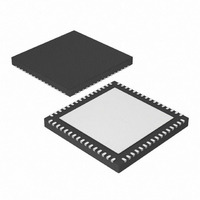
DSPIC33FJ64GS406-E/MR Microchip Technology, DSPIC33FJ64GS406-E/MR Datasheet - Page 333

DSPIC33FJ64GS406-E/MR
Manufacturer Part Number
DSPIC33FJ64GS406-E/MR
Description
MCU/DSP 16BIT 64KB FLASH 64QFN
Manufacturer
Microchip Technology
Series
dsPIC™ 33Fr
Datasheet
1.DSPIC33FJ32GS406-IPT.pdf
(418 pages)
Specifications of DSPIC33FJ64GS406-E/MR
Program Memory Type
FLASH
Program Memory Size
64KB (64K x 8)
Package / Case
64-VQFN
Core Processor
dsPIC
Core Size
16-Bit
Speed
40 MIPs
Connectivity
I²C, IrDA, LIN, SCI, SPI, UART/USART, USB
Peripherals
Brown-out Detect/Reset, QEI, POR, PWM, WDT
Number Of I /o
58
Ram Size
8K x 8
Voltage - Supply (vcc/vdd)
3 V ~ 3.6 V
Data Converters
A/D 16x10b
Oscillator Type
Internal
Operating Temperature
-40°C ~ 125°C
Product
DSCs
Data Bus Width
16 bit
Processor Series
DSPIC33F
Core
dsPIC
Numeric And Arithmetic Format
Fixed-Point or Floating-Point
Instruction Set Architecture
Harvard
Device Million Instructions Per Second
40 MIPs
Maximum Clock Frequency
120 MHz
Number Of Programmable I/os
58
Data Ram Size
4 KB
Operating Supply Voltage
3.3 V
Maximum Operating Temperature
+ 125 C
Mounting Style
SMD/SMT
3rd Party Development Tools
52713-733, 52714-737, 53276-922, EWDSPIC
Development Tools By Supplier
PG164130, DV164035, DV244005, DV164005, PG164120, DM240001, DV164033
Interface Type
I2C, SPI, UART
Minimum Operating Temperature
- 40 C
On-chip Adc
10 bit, 16 Channel
Lead Free Status / RoHS Status
Lead free / RoHS Compliant
Eeprom Size
-
Lead Free Status / Rohs Status
Lead free / RoHS Compliant
- Current page: 333 of 418
- Download datasheet (3Mb)
24.0
The
dsPIC33FJ64GS406/606/608/610
several features intended to maximize application
flexibility and reliability, and minimize cost through
elimination of external components. These are:
TABLE 24-1:
2010 Microchip Technology Inc.
0xF80000 FBS
0xF80002 RESERVED
0xF80004 FGS
0xF80006 FOSCSEL
0xF80008 FOSC
0xF8000A FWDT
0xF8000C FPOR
0xF8000E FICD
0xF80010 FCMP
Legend: — = unimplemented bit, read as ‘0’.
Note 1:
Address
dsPIC33FJ32GS406/606/608/610 and dsPIC33FJ64GS406/606/608/610
Note 1: This data sheet summarizes the features
2:
2: Some registers and associated bits
SPECIAL FEATURES
dsPIC33FJ32GS406/606/608/610
These bits are reserved for use by development tools and must be programmed as ‘1’.
These bits are reserved on dsPIC33FJXXXGS406 devices and always read as ‘1’.
of the dsPIC33FJ32GS406/606/608/610
and
devices. It is not intended to be a compre-
hensive reference source. To comple-
ment the information in this data sheet,
refer to the “dsPIC33F/PIC24H Family
Reference Manual”. Please see the
Microchip web site (www.microchip.com)
for the latest “dsPIC33F/PIC24H Family
Reference Manual” sections.
described in this section may not be avail-
able on all devices. Refer to Section 4.0
“Memory Organization” in this data
sheet for device-specific register and bit
information.
Name
DEVICE CONFIGURATION REGISTER MAP
dsPIC33FJ64GS406/606/608/610
Reserved
FWDTEN
IESO
Bit 7
—
—
—
—
—
FCKSM<1:0>
(1)
devices
Reserved
WINDIS
ALTQIO
Bit 6
—
—
—
—
—
include
(1)
and
Preliminary
CMPPOL1
JTAGEN
ALTSS1
Bit 5
—
—
—
—
—
—
(2)
• Flexible Configuration
• Watchdog Timer (WDT)
• Code Protection and CodeGuard™ Security
• JTAG Boundary Scan Interface
• In-Circuit Serial Programming™ (ICSP™)
• In-Circuit Emulation
• Brown-out Reset (BOR)
24.1
The Configuration bits can be programmed (read
as ‘0’), or left unprogrammed (read as ‘1’), to select
various device configurations. These bits are mapped
starting at program memory location 0xF80000.
The individual Configuration bit descriptions for the
Configuration registers are shown in Table 24-2.
Note that address, 0xF80000, is beyond the user pro-
gram memory space. It belongs to the configuration
memory space (0x800000-0xFFFFFF), which can only
be accessed using table reads and table writes.
The device Configuration register map is shown in
Table 24-1.
WDTPRE
Bit 4
HYST1<1:0>
—
—
—
—
—
—
Configuration Bits
—
Bit 3
—
—
—
—
—
(2)
CMPPOL0
BSS<2:0>
OSCIOFNC POSCMD<1:0>
WDTPOST<3:0>
Bit 2
—
—
GSS<1:0>
FNOSC<2:0>
FPWRT<2:0>
(2)
DS70591C-page 333
HYST0<1:0>
Bit 1
—
ICS<1:0>
GWRP
BWRP
Bit 0
—
(2)
Related parts for DSPIC33FJ64GS406-E/MR
Image
Part Number
Description
Manufacturer
Datasheet
Request
R

Part Number:
Description:
IC, DSC, 16BIT, 12KB, 40MHZ, 3.6V, DIP28
Manufacturer:
Microchip Technology
Datasheet:

Part Number:
Description:
Manufacturer:
Microchip Technology Inc.
Datasheet:

Part Number:
Description:
Manufacturer:
Microchip Technology Inc.
Datasheet:

Part Number:
Description:
Manufacturer:
Microchip Technology Inc.
Datasheet:

Part Number:
Description:
Manufacturer:
Microchip Technology Inc.
Datasheet:

Part Number:
Description:
Manufacturer:
Microchip Technology Inc.
Datasheet:

Part Number:
Description:
Manufacturer:
Microchip Technology Inc.
Datasheet:

Part Number:
Description:
Manufacturer:
Microchip Technology Inc.
Datasheet:

Part Number:
Description:
Manufacturer:
Microchip Technology Inc.
Datasheet:


