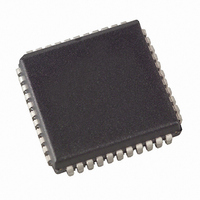
AT89S8253-24JU Atmel, AT89S8253-24JU Datasheet - Page 39

AT89S8253-24JU
Manufacturer Part Number
AT89S8253-24JU
Description
IC MCU 12K FLASH 24MHZ 44-PLCC
Manufacturer
Atmel
Series
89Sr
Datasheet
1.AT89S8253-24PU.pdf
(60 pages)
Specifications of AT89S8253-24JU
Core Processor
8051
Core Size
8-Bit
Speed
24MHz
Connectivity
SPI, UART/USART
Peripherals
POR, WDT
Number Of I /o
32
Program Memory Size
12KB (12K x 8)
Program Memory Type
FLASH
Eeprom Size
2K x 8
Ram Size
256 x 8
Voltage - Supply (vcc/vdd)
2.7 V ~ 5.5 V
Oscillator Type
Internal
Operating Temperature
-40°C ~ 85°C
Package / Case
44-PLCC
Processor Series
AT89x
Core
8051
Data Bus Width
8 bit
Data Ram Size
256 B
Interface Type
SPI/UART
Maximum Clock Frequency
24 MHz
Number Of Programmable I/os
32
Number Of Timers
3
Operating Supply Voltage
2.7 V to 5.5 V
Maximum Operating Temperature
+ 85 C
Mounting Style
SMD/SMT
3rd Party Development Tools
PK51, CA51, A51, ULINK2
Development Tools By Supplier
AT89ISP
Minimum Operating Temperature
- 40 C
Lead Free Status / RoHS Status
Lead free / RoHS Compliant
Data Converters
-
Lead Free Status / Rohs Status
Lead free / RoHS Compliant
Available stocks
Company
Part Number
Manufacturer
Quantity
Price
Company:
Part Number:
AT89S8253-24JU
Manufacturer:
LITTLEFUSE
Quantity:
4 500
Company:
Part Number:
AT89S8253-24JU
Manufacturer:
ATMEL
Quantity:
6
Company:
Part Number:
AT89S8253-24JU
Manufacturer:
ATMEL
Quantity:
5 530
Company:
Part Number:
AT89S8253-24JU
Manufacturer:
ATM
Quantity:
3 290
Company:
Part Number:
AT89S8253-24JU
Manufacturer:
ATMEL
Quantity:
44 616
Part Number:
AT89S8253-24JU
Manufacturer:
ATMEL/爱特梅尔
Quantity:
20 000
21. Programming Interface
22. Serial Downloading
23. Serial Programming Algorithm
3286P–MICRO–3/10
Every code byte in the Flash and EEPROM arrays can be written, and the entire array can be
erased, by using the appropriate combination of control signals. The write operation cycle is self-
timed and once initiated, will automatically time itself to completion.
Most worldwide major programming vendors offer support for the Atmel AT89 microcontroller
series. Please contact your local programming vendor for the appropriate software revision.
Both the code and data memory arrays can be programmed using the serial SPI bus while RST
is pulled to V
RST is set high, the Programming Enable instruction must be executed first before other opera-
tions can be executed.
The Chip Erase operation turns the content of every memory location in both the Code and Data
arrays into FFH.
The code and data memory arrays have separate address spaces:
Either an external system clock is supplied at pin XTAL1 or a crystal needs to be connected
across pins XTAL1 and XTAL2. The maximum serial clock (SCK) frequency should be less than
1/16 of the crystal frequency. With a 24 MHz oscillator clock, the maximum SCK frequency is
1.5 MHz.
To program and verify the AT89S8253 in the serial programming mode, the following sequence
is recommended:
If a crystal is not connected across pins XTAL1 and XTAL2, apply a 3 MHz to 12 MHz clock to
XTAL1 pin and wait for at least 10 ms with RST pin high and P1.7 (SCK) low.
Power-off sequence (if needed):
1. Power-up sequence:
2. Enable serial programming by sending the Programming Enable serial instruction to pin
3. The code or data array is programmed one byte or one page at a time by supplying the
4. Any memory location can be verified by using the Read instruction which returns the
5. At the end of a programming session, RST can be set low to commence normal
1. Set XTAL1 to “L” (if a crystal is not used).
2. Set RST to “L”.
3. Turn V
0000H to 2FFFH for code memory and 000H to 7FFH for data memory.
a. Apply power between VCC and GND pins.
b. Set RST pin to “H”.
MOSI/P1.5. The frequency of the shift clock supplied at pin SCK/P1.7 needs to be less
than the CPU clock at XTAL1 divided by 16.
address and data together with the appropriate Write instruction. The write cycle is self-
timed and typically takes less than 4.0 ms at 5V.
content at the selected address at serial output MISO/P1.6.
operation.
CC
CC
. The serial interface consists of pins SCK, MOSI (input) and MISO (output). After
power off.
AT89S8253
39


