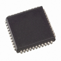
AT89C51CC01UA-SLSUM Atmel, AT89C51CC01UA-SLSUM Datasheet - Page 5

AT89C51CC01UA-SLSUM
Manufacturer Part Number
AT89C51CC01UA-SLSUM
Description
IC 8051 MCU FLASH 32K 44-PLCC
Manufacturer
Atmel
Series
AT89C CANr
Datasheet
1.T89C51CC01CA-7CTIM.pdf
(167 pages)
Specifications of AT89C51CC01UA-SLSUM
Core Processor
8051
Core Size
8-Bit
Speed
40MHz
Connectivity
CAN, UART/USART
Peripherals
POR, PWM, WDT
Number Of I /o
34
Program Memory Size
32KB (32K x 8)
Program Memory Type
FLASH
Eeprom Size
2K x 8
Ram Size
1.25K x 8
Voltage - Supply (vcc/vdd)
3 V ~ 5.5 V
Data Converters
A/D 8x10b
Oscillator Type
External
Operating Temperature
-40°C ~ 85°C
Package / Case
44-PLCC
Package
44PLCC
Device Core
8051
Family Name
89C
Maximum Speed
40 MHz
Operating Supply Voltage
3.3|5 V
Data Bus Width
8 Bit
Number Of Programmable I/os
34
Interface Type
CAN/UART
On-chip Adc
8-chx10-bit
Number Of Timers
3
Processor Series
AT89x
Core
8051
Data Ram Size
1280 B
Maximum Clock Frequency
40 MHz
Maximum Operating Temperature
+ 85 C
Mounting Style
SMD/SMT
3rd Party Development Tools
PK51, CA51, A51, ULINK2
Development Tools By Supplier
CANADAPT28
Minimum Operating Temperature
- 40 C
Cpu Family
AT89
Device Core Size
8b
Frequency (max)
40MHz
Total Internal Ram Size
1.25KB
# I/os (max)
34
Number Of Timers - General Purpose
3
Operating Supply Voltage (typ)
3.3/5V
Operating Supply Voltage (max)
5.5V
Operating Supply Voltage (min)
3V
Instruction Set Architecture
CISC
Operating Temp Range
-40C to 85C
Operating Temperature Classification
Industrial
Mounting
Surface Mount
Pin Count
44
Package Type
PLCC
For Use With
AT89OCD-01 - USB EMULATOR FOR AT8XC51 MCU
Lead Free Status / RoHS Status
Lead free / RoHS Compliant
Other names
AT89C51CC01UASLSUM
Available stocks
Company
Part Number
Manufacturer
Quantity
Price
Company:
Part Number:
AT89C51CC01UA-SLSUM
Manufacturer:
ATMEL
Quantity:
678
Read-Modify-Write
Instructions
4129N–CAN–03/08
Figure 2. Port 0 Structure
Notes:
Figure 3. Port 2 Structure
Notes:
When Port 0 and Port 2 are used for an external memory cycle, an internal control signal
switches the output-driver input from the latch output to the internal address/data line.
Some instructions read the latch data rather than the pin data. The latch based instruc-
tions read the data, modify the data and then rewrite the latch. These are called "Read-
Modify-Write" instructions. Below is a complete list of these special instructions (see
Table ). When the destination operand is a Port or a Port bit, these instructions read the
latch rather than the pin:
READ
LATCH
INTERNAL
BUS
WRITE
TO
LATCH
READ
PIN
READ
LATCH
INTERNAL
BUS
WRITE
TO
LATCH
READ
PIN
1. Port 0 is precluded from use as general-purpose I/O Ports when used as
2. Port 0 internal strong pull-ups assist the logic-one output for memory bus cycles only.
1. Port 2 is precluded from use as general-purpose I/O Ports when as address/data bus
2. Port 2 internal strong pull-ups FET (P1 in FiGURE) assist the logic-one output for
address/data bus drivers.
Except for these bus cycles, the pull-up FET is off, Port 0 outputs are open-drain.
drivers.
memory bus cycle.
D
LATCH
P0.X
D
LATCH
P2.X
ADDRESS LOW/
DATA
Q
ADDRESS HIGH/ CONTROL
Q
CONTROL
1
0
1
0
VDD
VDD
(2)
INTERNAL
PULL-UP (2)
P0.x (1)
P2.x (1)
5


