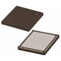
PIC24FJ128GB206-I/MR Microchip Technology, PIC24FJ128GB206-I/MR Datasheet - Page 25

PIC24FJ128GB206-I/MR
Manufacturer Part Number
PIC24FJ128GB206-I/MR
Description
MCU PIC 16BIT FLASH USB 64VQFN
Manufacturer
Microchip Technology
Series
PIC® 24Fr
Specifications of PIC24FJ128GB206-I/MR
Core Size
16-Bit
Program Memory Size
128KB (43K x 24)
Core Processor
PIC
Speed
32MHz
Connectivity
I²C, IrDA, SPI, UART/USART, USB OTG
Peripherals
Brown-out Detect/Reset, LVD, POR, PWM, WDT
Number Of I /o
52
Program Memory Type
FLASH
Ram Size
96K x 8
Voltage - Supply (vcc/vdd)
2.2 V ~ 3.6 V
Data Converters
A/D 16x10b
Oscillator Type
Internal
Operating Temperature
-40°C ~ 85°C
Package / Case
64-VFQFN, Exposed Pad
Controller Family/series
PIC24
No. Of I/o's
52
Ram Memory Size
96KB
Cpu Speed
32MHz
No. Of Timers
5
No. Of Pwm Channels
9
Processor Series
PIC24FJ
Core
PIC
Data Bus Width
16 bit
Data Ram Size
96 KB
Interface Type
I2C, SPI, UART
Maximum Clock Frequency
32 MHz
Number Of Programmable I/os
29
Number Of Timers
5
Operating Supply Voltage
2.2 V to 3.6 V
Maximum Operating Temperature
+ 85 C
Mounting Style
SMD/SMT
3rd Party Development Tools
52713-733, 52714-737, 53276-922, EWDSPIC
Development Tools By Supplier
PG164130, DV164035, DV244005, DV164005, DM240001, MA240021
Minimum Operating Temperature
- 40 C
On-chip Adc
10 bit, 16 Channel
Lead Free Status / RoHS Status
Lead free / RoHS Compliant
Eeprom Size
-
Lead Free Status / Rohs Status
Details
- Current page: 25 of 386
- Download datasheet (4Mb)
TABLE 1-3:
2010 Microchip Technology Inc.
PMD0
PMD1
PMD2
PMD3
PMD4
PMD5
PMD6
PMD7
PMD8
PMD9
PMD10
PMD11
PMD12
PMD13
PMD14
PMD15
PMRD
PMWR
RA0
RA1
RA2
RA3
RA4
RA5
RA6
RA7
RA9
RA10
RA14
RA15
Legend:
Note 1:
Function
2:
3:
4:
TTL = TTL input buffer
ANA = Analog level input/output
The alternate EPMP pins are selected when the ALTPMP (CW3<12>) bit is programmed to ‘0’.
The PMSC2 signal will replace the PMA15 signal on the 15-pin PMA when CSF<1:0> = 01 or 10.
The PMCS1 signal will replace the PMA14 signal on the 14-pin PMA when CSF<1:0> = 10.
The alternate V
TQFP/QFN
64-Pin
60
61
62
63
64
53
52
—
—
—
—
—
—
—
—
—
—
—
—
—
—
—
—
—
—
—
—
1
2
3
PIC24FJ256GB210 FAMILY PINOUT DESCRIPTIONS (CONTINUED)
Pin Number
REF
100-Pin
TQFP
pins selected when the ALTVREF (CW1<5>) bit is programmed to ‘0’.
100
93
94
98
99
90
89
88
87
79
80
83
84
82
81
17
38
58
59
60
61
91
92
28
29
66
67
3
4
5
121-Pin
BGA
G10
G11
H11
E11
G3
G9
A4
B4
B3
A2
A1
D3
C1
D2
A5
E6
A6
B6
A9
D8
D7
C7
B8
C8
C5
B5
K3
E8
J6
L2
PIC24FJ256GB210 FAMILY
I/O
I/O
I/O
I/O
I/O
I/O
I/O
I/O
I/O
I/O
I/O
I/O
I/O
I/O
I/O
I/O
I/O
I/O
I/O
I/O
I/O
I/O
I/O
I/O
I/O
I/O
I/O
I/O
I/O
I/O
I/O
ST/TTL
ST/TTL
ST/TTL
ST/TTL
ST/TTL
ST/TTL
ST/TTL
ST/TTL
ST/TTL
ST/TTL
ST/TTL
ST/TTL
ST/TTL
ST/TTL
ST/TTL
ST/TTL
ST/TTL Parallel Master Port Read Strobe.
ST/TTL Parallel Master Port Write Strobe.
Buffer
Input
ST
ST
ST
ST
ST
ST
ST
ST
ST
ST
ST
ST
ST = Schmitt Trigger input buffer
I
2
C™ = I
Parallel Master Port Data bits<15:0>.
PORTA Digital I/O.
2
C/SMBus input buffer
Description
DS39975A-page 25
Related parts for PIC24FJ128GB206-I/MR
Image
Part Number
Description
Manufacturer
Datasheet
Request
R

Part Number:
Description:
64/80/100-Pin, 16-Bit Flash Microcontrollers with USB On-The-Go (OTG)
Manufacturer:
MICROCHIP [Microchip Technology]
Datasheet:

Part Number:
Description:
Manufacturer:
Microchip Technology Inc.
Datasheet:

Part Number:
Description:
Manufacturer:
Microchip Technology Inc.
Datasheet:

Part Number:
Description:
Manufacturer:
Microchip Technology Inc.
Datasheet:

Part Number:
Description:
Manufacturer:
Microchip Technology Inc.
Datasheet:

Part Number:
Description:
Manufacturer:
Microchip Technology Inc.
Datasheet:

Part Number:
Description:
Manufacturer:
Microchip Technology Inc.
Datasheet:

Part Number:
Description:
Manufacturer:
Microchip Technology Inc.
Datasheet:

Part Number:
Description:
Manufacturer:
Microchip Technology Inc.
Datasheet:


