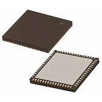
PIC24FJ128GB206-I/MR Microchip Technology, PIC24FJ128GB206-I/MR Datasheet - Page 88

PIC24FJ128GB206-I/MR
Manufacturer Part Number
PIC24FJ128GB206-I/MR
Description
MCU PIC 16BIT FLASH USB 64VQFN
Manufacturer
Microchip Technology
Series
PIC® 24Fr
Specifications of PIC24FJ128GB206-I/MR
Core Size
16-Bit
Program Memory Size
128KB (43K x 24)
Core Processor
PIC
Speed
32MHz
Connectivity
I²C, IrDA, SPI, UART/USART, USB OTG
Peripherals
Brown-out Detect/Reset, LVD, POR, PWM, WDT
Number Of I /o
52
Program Memory Type
FLASH
Ram Size
96K x 8
Voltage - Supply (vcc/vdd)
2.2 V ~ 3.6 V
Data Converters
A/D 16x10b
Oscillator Type
Internal
Operating Temperature
-40°C ~ 85°C
Package / Case
64-VFQFN, Exposed Pad
Controller Family/series
PIC24
No. Of I/o's
52
Ram Memory Size
96KB
Cpu Speed
32MHz
No. Of Timers
5
No. Of Pwm Channels
9
Processor Series
PIC24FJ
Core
PIC
Data Bus Width
16 bit
Data Ram Size
96 KB
Interface Type
I2C, SPI, UART
Maximum Clock Frequency
32 MHz
Number Of Programmable I/os
29
Number Of Timers
5
Operating Supply Voltage
2.2 V to 3.6 V
Maximum Operating Temperature
+ 85 C
Mounting Style
SMD/SMT
3rd Party Development Tools
52713-733, 52714-737, 53276-922, EWDSPIC
Development Tools By Supplier
PG164130, DV164035, DV244005, DV164005, DM240001, MA240021
Minimum Operating Temperature
- 40 C
On-chip Adc
10 bit, 16 Channel
Lead Free Status / RoHS Status
Lead free / RoHS Compliant
Eeprom Size
-
Lead Free Status / Rohs Status
Details
- Current page: 88 of 386
- Download datasheet (4Mb)
PIC24FJ256GB210 FAMILY
6.1
Most of the Special Function Registers (SFRs) associ-
ated with the PIC24F CPU and peripherals are reset to a
particular value at a device Reset. The SFRs are
grouped by their peripheral or CPU function and their
Reset values are specified in each section of this manual.
The Reset value for each SFR does not depend on the
type of Reset, with the exception of four registers. The
Reset value for the Reset Control register, RCON, will
depend on the type of device Reset. The Reset value
for the Oscillator Control register, OSCCON, will
depend on the type of Reset and the programmed
values of the FNOSC bits in Flash Configuration
Word 2 (CW2) (see Table 6-2). The RCFGCAL and
NVMCON registers are only affected by a POR.
6.2
The Reset times for various types of device Reset are
summarized in Table 6-3. Note that the system Reset
signal, SYSRST, is released after the POR delay time
expires.
The time at which the device actually begins to execute
code will also depend on the system oscillator delays,
which include the Oscillator Start-up Timer (OST) and
the PLL lock time. The OST and PLL lock times occur
in parallel with the applicable SYSRST delay times.
The Fail-Safe Clock Monitor (FSCM) delay determines
the time at which the FSCM begins to monitor the
system clock source after the SYSRST signal is
released.
DS39975A-page 88
Special Function Register Reset
States
Device Reset Times
6.3
If clock switching is enabled, the system clock source at
device Reset is chosen, as shown in Table 6-2. If clock
switching is disabled, the system clock source is always
selected according to the oscillator Configuration bits.
Refer to Section 8.0 “Oscillator Configuration” for
further details.
TABLE 6-2:
Reset Type
WDTO
MCLR
SWR
POR
BOR
Clock Source Selection at Reset
FNOSC Configuration bits
(CW2<10:8>)
COSC Control bits
(OSCCON<14:12>)
OSCILLATOR SELECTION vs.
TYPE OF RESET (CLOCK
SWITCHING ENABLED)
Clock Source Determinant
2010 Microchip Technology Inc.
Related parts for PIC24FJ128GB206-I/MR
Image
Part Number
Description
Manufacturer
Datasheet
Request
R

Part Number:
Description:
64/80/100-Pin, 16-Bit Flash Microcontrollers with USB On-The-Go (OTG)
Manufacturer:
MICROCHIP [Microchip Technology]
Datasheet:

Part Number:
Description:
Manufacturer:
Microchip Technology Inc.
Datasheet:

Part Number:
Description:
Manufacturer:
Microchip Technology Inc.
Datasheet:

Part Number:
Description:
Manufacturer:
Microchip Technology Inc.
Datasheet:

Part Number:
Description:
Manufacturer:
Microchip Technology Inc.
Datasheet:

Part Number:
Description:
Manufacturer:
Microchip Technology Inc.
Datasheet:

Part Number:
Description:
Manufacturer:
Microchip Technology Inc.
Datasheet:

Part Number:
Description:
Manufacturer:
Microchip Technology Inc.
Datasheet:

Part Number:
Description:
Manufacturer:
Microchip Technology Inc.
Datasheet:


