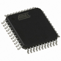
AT89C51CC03UA-RLTUM Atmel, AT89C51CC03UA-RLTUM Datasheet - Page 50

AT89C51CC03UA-RLTUM
Manufacturer Part Number
AT89C51CC03UA-RLTUM
Description
IC 8051 MCU 64K FLASH 44-VQFP
Manufacturer
Atmel
Series
AT89C CANr
Datasheet
1.AT89C51CC03C-S3RIM.pdf
(198 pages)
Specifications of AT89C51CC03UA-RLTUM
Core Processor
8051
Core Size
8-Bit
Speed
40MHz
Connectivity
CAN, UART/USART
Peripherals
POR, PWM, WDT
Number Of I /o
36
Program Memory Size
64KB (64K x 8)
Program Memory Type
FLASH
Eeprom Size
2K x 8
Ram Size
2.25K x 8
Voltage - Supply (vcc/vdd)
3 V ~ 5.5 V
Data Converters
A/D 8x10b
Oscillator Type
External
Operating Temperature
-40°C ~ 85°C
Package / Case
44-TQFP, 44-VQFP
Package
44VQFP
Device Core
8051
Family Name
89C
Maximum Speed
60 MHz
Operating Supply Voltage
5 V
Data Bus Width
8 Bit
Number Of Programmable I/os
36
Interface Type
CAN/SPI/UART
On-chip Adc
8-chx10-bit
Number Of Timers
3
Processor Series
AT89x
Core
8051
Data Ram Size
2304 B
Maximum Clock Frequency
60 MHz
Maximum Operating Temperature
+ 85 C
Mounting Style
SMD/SMT
3rd Party Development Tools
PK51, CA51, A51, ULINK2
Minimum Operating Temperature
- 40 C
Cpu Family
AT89
Device Core Size
8b
Frequency (max)
60MHz
Total Internal Ram Size
2.25KB
# I/os (max)
36
Number Of Timers - General Purpose
3
Operating Supply Voltage (typ)
5V
Operating Supply Voltage (max)
5.5V
Operating Supply Voltage (min)
4.5V
Instruction Set Architecture
CISC
Operating Temp Range
-40C to 85C
Operating Temperature Classification
Industrial
Mounting
Surface Mount
Pin Count
44
Package Type
VQFP
For Use With
AT89OCD-01 - USB EMULATOR FOR AT8XC51 MCU
Lead Free Status / RoHS Status
Lead free / RoHS Compliant
Available stocks
Company
Part Number
Manufacturer
Quantity
Price
Programming the Flash Spaces
User
Extra Row
50
AT89C51CC03
Figure 25. Column Latches Loading Procedure
Note:
The following procedure is used to program the User space and is summarized in
Figure 26:
•
•
•
•
The following procedure is used to program the Extra Row space and is summarized in
Figure 26:
•
•
•
•
Load up to one page of data in the column latches from address 0000h to FFFFh.
Save and Disable the interrupts.
Launch the programming by writing the data sequence 50h followed by A0h in
FCON register (only from FM1).
The end of the programming indicated by the FBUSY flag cleared.
Restore the interrupts.
Load data in the column latches from address FF80h to FFFFh.
Save and Disable the interrupts.
Launch the programming by writing the data sequence 52h followed by A2h in
FCON register (only from FM1).
The end of the programming indicated by the FBUSY flag cleared.
Restore the interrupts.
The last page address used when loading the column latch is the one used to select the
page programming address.
Column Latches Mapping
Exec: MOVX @DPTR, A
Data memory Mapping
FCON = 00h (FPS = 0)
FCON = 08h (FPS=1)
Column Latches
Save and Disable IT
DPTR = Address
ACC = Data
Last Byte
Data Load
to load?
Restore IT
Loading
EA = 0
4182O–CAN–09/08


