EP7309-CVZ Cirrus Logic Inc, EP7309-CVZ Datasheet - Page 3
EP7309-CVZ
Manufacturer Part Number
EP7309-CVZ
Description
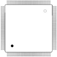
IC ARM720T MCU 74MHZ 208-LQFP
Manufacturer
Cirrus Logic Inc
Series
EP7r
Specifications of EP7309-CVZ
Core Size
32-Bit
Core Processor
ARM7
Speed
74MHz
Connectivity
Codec, DAI, EBI/EMI, IrDA, Keypad, SPI/Microwire1, UART/USART
Peripherals
LCD, LED, MaverickKey, POR, PWM
Number Of I /o
27
Program Memory Type
ROMless
Ram Size
56K x 8
Voltage - Supply (vcc/vdd)
2.3 V ~ 2.7 V
Oscillator Type
External
Operating Temperature
0°C ~ 70°C
Package / Case
208-LQFP
Controller Family/series
(ARM7)
No. Of I/o's
27
Ram Memory Size
48KB
Cpu Speed
74MHz
No. Of Timers
2
No. Of Pwm Channels
2
Digital Ic Case Style
LQFP
Embedded Interface Type
SSI, UART
Rohs Compliant
Yes
Processor Series
EP73xx
Core
ARM720T
Data Bus Width
32 bit
Mounting Style
SMD/SMT
3rd Party Development Tools
MDK-ARM, RL-ARM, ULINK2
Lead Free Status / RoHS Status
Lead free / RoHS Compliant
Eeprom Size
-
Program Memory Size
-
Data Converters
-
Lead Free Status / Rohs Status
Details
Other names
598-1214
Available stocks
Company
Part Number
Manufacturer
Quantity
Price


Table of Contents
FEATURES
OVERVIEW
ELECTRICAL SPECIFICATIONS ......................................................................................................12
Timings ...............................................................................................................................................14
Packages ............................................................................................................................................24
DS507F1
Processor Core - ARM720T ..................................................................................................................................6
Power Management ..............................................................................................................................................6
MaverickKey™ Unique ID ......................................................................................................................................6
Memory Interfaces .................................................................................................................................................6
Digital Audio Capability .........................................................................................................................................6
Universal Asynchronous Receiver/Transmitters (UARTs) .....................................................................................6
Digital Audio Interface (DAI) ..................................................................................................................................7
CODEC Interface ..................................................................................................................................................7
SSI2 Interface ........................................................................................................................................................7
Synchronous Serial Interface ................................................................................................................................8
LCD Controller .......................................................................................................................................................8
Interrupt Controller ................................................................................................................................................8
Real-Time Clock ....................................................................................................................................................8
PLL and Clocking ..................................................................................................................................................9
DC-to-DC converter interface (PWM) ....................................................................................................................9
Timers ...................................................................................................................................................................9
General Purpose Input/Output (GPIO) ..................................................................................................................9
Hardware debug Interface .....................................................................................................................................9
Internal Boot ROM ...............................................................................................................................................10
Packaging ............................................................................................................................................................10
Pin Multiplexing ...................................................................................................................................................10
System Design ....................................................................................................................................................11
Absolute Maximum Ratings .................................................................................................................................12
Recommended Operating Conditions .................................................................................................................12
DC Characteristics ..............................................................................................................................................12
Static Memory .....................................................................................................................................................15
SSI1 Interface ......................................................................................................................................................20
SSI2 Interface ......................................................................................................................................................21
LCD Interface ......................................................................................................................................................22
JTAG Interface .....................................................................................................................................................23
208-Pin LQFP Package Characteristics ..............................................................................................................24
204-Ball TFBGA Package Characteristics ...........................................................................................................29
Timing Diagram Conventions ....................................................................................................................14
Timing Conditions ......................................................................................................................................14
Static Memory Single Read Cycle .............................................................................................................16
Static Memory Single Write Cycle .............................................................................................................17
Static Memory Burst Read Cycle ...............................................................................................................18
Static Memory Burst Write Cycle ...............................................................................................................19
208-Pin LQFP Package Specifications ......................................................................................................24
208-Pin LQFP Pin Diagram .......................................................................................................................25
208-Pin LQFP Numeric Pin Listing ............................................................................................................26
204-Ball TFBGA Package Specifications ..................................................................................................29
204-Ball TFBGA Pinout (Top View) ...........................................................................................................30
...................................................................................................................................................................1
..................................................................................................................................................................1
©
Copyright Cirrus Logic, Inc. 2005
(All Rights Reserved)
High-Performance, Low-Power System on Chip
EP7309
3
Related parts for EP7309-CVZ
Image
Part Number
Description
Manufacturer
Datasheet
Request
R

Part Number:
Description:
IC ARM720T MCU 74MHZ 256-PBGA
Manufacturer:
Cirrus Logic Inc
Datasheet:

Part Number:
Description:
32-Bit Microcontroller IC
Manufacturer:
Cirrus Logic Inc
Datasheet:
Part Number:
Description:
IC, 32BIT MCU, ARM7, 74MHZ, BGA-256
Manufacturer:
Cirrus Logic Inc
Part Number:
Description:
IC, 32BIT MCU, ARM7, 74MHZ, LQFP-208
Manufacturer:
Cirrus Logic Inc

Part Number:
Description:
Development Kit
Manufacturer:
Cirrus Logic Inc
Datasheet:
Part Number:
Description:
Development Kit
Manufacturer:
Cirrus Logic Inc
Datasheet:


Part Number:
Description:
High-efficiency PFC + Fluorescent Lamp Driver Reference Design
Manufacturer:
Cirrus Logic Inc
Datasheet:
Part Number:
Description:
Development Kit
Manufacturer:
Cirrus Logic Inc
Datasheet:
Part Number:
Description:
Development Kit
Manufacturer:
Cirrus Logic Inc
Datasheet:

Part Number:
Description:
Development Kit
Manufacturer:
Cirrus Logic Inc
Datasheet:
Part Number:
Description:
Development Kit
Manufacturer:
Cirrus Logic Inc
Datasheet:

Part Number:
Description:
Ref Bd For Speakerbar MSA & DSP Products
Manufacturer:
Cirrus Logic Inc