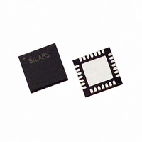
C8051F311-GMR Silicon Laboratories Inc, C8051F311-GMR Datasheet - Page 81

C8051F311-GMR
Manufacturer Part Number
C8051F311-GMR
Description
IC 8051 MCU 16K FLASH 28MLP
Manufacturer
Silicon Laboratories Inc
Series
C8051F31xr
Specifications of C8051F311-GMR
Core Processor
8051
Core Size
8-Bit
Speed
25MHz
Connectivity
SMBus (2-Wire/I²C), SPI, UART/USART
Peripherals
POR, PWM, Temp Sensor, WDT
Number Of I /o
25
Program Memory Size
16KB (16K x 8)
Program Memory Type
FLASH
Ram Size
1.25K x 8
Voltage - Supply (vcc/vdd)
2.7 V ~ 3.6 V
Data Converters
A/D 17x10b
Oscillator Type
Internal
Operating Temperature
-40°C ~ 85°C
Package / Case
28-VQFN Exposed Pad, 28-HVQFN, 28-SQFN, 28-DHVQFN
Package
24QFN EP
Device Core
8051
Family Name
C8051F31x
Maximum Speed
25 MHz
Operating Supply Voltage
3.3 V
Data Bus Width
8 Bit
Number Of Programmable I/os
25
Interface Type
I2C/SMBus/SPI/UART
On-chip Adc
17-chx10-bit
Number Of Timers
4
For Use With
336-1446 - ADAPTER PROGRAM TOOLSTICK F311336-1253 - DEV KIT FOR C8051F310/F311
Lead Free Status / RoHS Status
Lead free / RoHS Compliant
Eeprom Size
-
Available stocks
Company
Part Number
Manufacturer
Quantity
Price
Part Number:
C8051F311-GMR
Manufacturer:
SILICON LABS/芯科
Quantity:
20 000
CIP-51 Instruction Set Summary, which includes the mnemonic, number of bytes, and number of clock
cycles for each instruction.
8.1.2. MOVX Instruction and Program Memory
The MOVX instruction is typically used to access external data memory (Note: the C8051F31x does not
support external data or program memory). In the CIP-51, the MOVX write instruction is used to accesses
external RAM and the on-chip program memory space implemented as re-programmable Flash memory.
The Flash access feature provides a mechanism for the CIP-51 to update program code and use the pro-
gram memory space for non-volatile data storage. Refer to
further details.
Mnemonic
ADD A, Rn
ADD A, direct
ADD A, @Ri
ADD A, #data
ADDC A, Rn
ADDC A, direct
ADDC A, @Ri
ADDC A, #data
SUBB A, Rn
SUBB A, direct
SUBB A, @Ri
SUBB A, #data
INC A
INC Rn
INC direct
INC @Ri
DEC A
DEC Rn
DEC direct
DEC @Ri
INC DPTR
MUL AB
DIV AB
DA A
ANL A, Rn
ANL A, direct
ANL A, @Ri
ANL A, #data
ANL direct, A
ANL direct, #data
ORL A, Rn
Table 8.1. CIP-51 Instruction Set Summary
Description
Add register to A
Add direct byte to A
Add indirect RAM to A
Add immediate to A
Add register to A with carry
Add direct byte to A with carry
Add indirect RAM to A with carry
Add immediate to A with carry
Subtract register from A with borrow
Subtract direct byte from A with borrow
Subtract indirect RAM from A with borrow
Subtract immediate from A with borrow
Increment A
Increment register
Increment direct byte
Increment indirect RAM
Decrement A
Decrement register
Decrement direct byte
Decrement indirect RAM
Increment Data Pointer
Multiply A and B
Divide A by B
Decimal adjust A
AND Register to A
AND direct byte to A
AND indirect RAM to A
AND immediate to A
AND A to direct byte
AND immediate to direct byte
OR Register to A
Arithmetic Operations
Logical Operations
Rev. 1.7
C8051F310/1/2/3/4/5/6/7
Section “10. Flash Memory” on page 111
Bytes
1
2
1
2
1
2
1
2
1
2
1
2
1
1
2
1
1
1
2
1
1
1
1
1
1
2
1
2
2
3
1
Cycles
Clock
1
2
2
2
1
2
2
2
1
2
2
2
1
1
2
2
1
1
2
2
1
4
8
1
1
2
2
2
2
3
1
for
81


