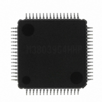
M38039G4HHP#U0 Renesas Electronics America, M38039G4HHP#U0 Datasheet - Page 84

M38039G4HHP#U0
Manufacturer Part Number
M38039G4HHP#U0
Description
IC 740/3803 MCU QZROM 64LQFP
Manufacturer
Renesas Electronics America
Series
740/38000r
Datasheet
1.M38039G4HHPU0.pdf
(105 pages)
Specifications of M38039G4HHP#U0
Core Processor
740
Core Size
8-Bit
Speed
16.8MHz
Connectivity
SIO, UART/USART
Peripherals
LED, PWM, WDT
Number Of I /o
56
Program Memory Size
16KB (16K x 8)
Program Memory Type
QzROM
Ram Size
2K x 8
Voltage - Supply (vcc/vdd)
1.8 V ~ 5.5 V
Data Converters
A/D 16x10b; D/A 2x8b
Oscillator Type
Internal
Operating Temperature
-20°C ~ 85°C
Package / Case
64-LQFP
Lead Free Status / RoHS Status
Lead free / RoHS Compliant
Eeprom Size
-
Available stocks
Company
Part Number
Manufacturer
Quantity
Price
3803 Group (Spec.H QzROM version)
REJ03B0166-0113 Rev.1.13
Page 82 of 100
Notes on Interrupts
1. Change of relevant register settings
When the setting of the following registers or bits is changed, the
interrupt request bit may be set to “1”. When not requiring the
interrupt occurrence synchronized with these setting, take the
following sequence.
• Interrupt edge selection register (address 003A
• Timer XY mode register (address 0023
• Timer Z mode register (address 002A
Set the above listed registers or bits as the following sequence.
Fig 80. Sequence of changing relevant register
<Reason>
The interrupt request bit may be set to “1” in the following cases.
• When setting the external interrupt active edge
Related bits:
INT
(bit 0 of interrupt edge selection register (address 003A
INT
(bit 1 of interrupt edge selection register (address 003A
INT
(bit 3 of interrupt edge selection register (address 003A
INT
(bit 4 of interrupt edge selection register (address 003A
INT
(bit 5 of interrupt edge selection register (address 003A
CNTR
(bit 2 of timer XY mode register (address 0023
CNTR
(bits 6 of timer XY mode register (address 0023
CNTR
(bits 5 of timer Z mode register (address 002A
Set the corresponding interrupt enable bit to “0” (disabled).
Set the corresponding interrupt enable bit to “1” (enabled).
Set the interrupt edge select bit (active edge switch bit)
or the interrupt (source) select bit to “1”.
0
1
2
3
4
interrupt edge selection bit
interrupt edge selection bit
interrupt edge selection bit
interrupt edge selection bit
interrupt edge selection bit
Set the corresponding interrupt request bit to “0”
0
1
2
activate edge switch bit
activate edge switch bit
activate edge switch bit
NOP (one or more instructions)
(no interrupt request issued).
Aug 21, 2009
16
16
)
)
16
16
16
16
))
)
))
))
16
16
16
16
16
))
))
))
))
))
• When switching the interrupt sources of an interrupt vector
2. Check of interrupt request bit
When executing the BBC or BBS instruction to an interrupt
request bit of an interrupt request register immediately after this
bit is set to “0”, execute one or more instructions before
executing the BBC or BBS instruction.
Fig 81. Sequence of check of interrupt request bit
<Reason>
If the BBC or BBS instruction is executed immediately after an
interrupt request bit of an interrupt request register is cleared to
“0”, the value of the interrupt request bit before being cleared to
“0” is read.
Notes on 8-bit Timer (timer 1, 2, X, Y)
• If a value n (between 0 and 255) is written to a timer latch, the
• When switching the count source by the timer 12, X and Y
• Set the double-function port of the CNTR
• Set the double-function port of CNTR
address where two or more interrupt sources are assigned
Related bits:
INT
(bit 6 of interrupt edge selection register (address 003A
INT
(bit 0 of interrupt source selection register (address 0039
Serial I/O2/Timer Z interrupt source selection bit
(bit 1 of interrupt source selection register (address 0039
INT
(bit 4 of interrupt source selection register (address 0039
CNTR
(bit 6 of interrupt source selection register (address 0039
AD conversion/Serial I/O3 transmit interrupt source selection bit
(bit 6 of interrupt source selection register (address 0039
frequency division ratio is 1/(n+1).
count source selection bits, the value of timer count is altered
in unconsiderable amount owing to generating of thin pulses in
the count input signals.
Therefore, select the timer count source before set the value to
the prescaler and the timer.
port P5
P5
measurement mode.
Clear the interrupt request bit to “0” (no interrupt issued)
4
/P5
0
0
4
, INT
/Timer Z interrupt source selection bit
/CNTR
1
5
4
/Serial I/O3 receive interrupt source selection bit
/P5
to input in the event counter mode and the pulse width
4
5
Execute the BBC or BBS instruction
interrupt switch bit
2
to output in the pulse output mode.
interrupt source selection bit
NOP (one or more instructions)
0
/CNTR
0
/CNTR
1
pin and port
1
pin and
16
16
16
16
16
16
))
))
))
))
))
))


