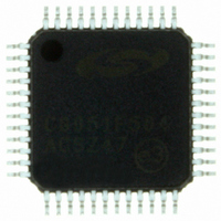
C8051F504-IQ Silicon Laboratories Inc, C8051F504-IQ Datasheet - Page 98

C8051F504-IQ
Manufacturer Part Number
C8051F504-IQ
Description
IC 8051 MCU 32K FLASH 48-QFP
Manufacturer
Silicon Laboratories Inc
Series
C8051F50xr
Specifications of C8051F504-IQ
Program Memory Type
FLASH
Program Memory Size
32KB (32K x 8)
Package / Case
48-QFP
Mfg Application Notes
LIN Bootloader AppNote
Core Processor
8051
Core Size
8-Bit
Speed
50MHz
Connectivity
EBI/EMI, SMBus (2-Wire/I²C), CAN, LIN, SPI, UART/USART
Peripherals
POR, PWM, Temp Sensor, WDT
Number Of I /o
40
Ram Size
4.25K x 8
Voltage - Supply (vcc/vdd)
1.8 V ~ 5.25 V
Data Converters
A/D 32x12b
Oscillator Type
Internal
Operating Temperature
-40°C ~ 125°C
Processor Series
C8051F5x
Core
8051
Data Bus Width
8 bit
Data Ram Size
4.25 KB
Interface Type
I2C/SPI/UART
Maximum Clock Frequency
50 MHz
Number Of Programmable I/os
40
Number Of Timers
4
Maximum Operating Temperature
+ 125 C
Mounting Style
SMD/SMT
3rd Party Development Tools
PK51, CA51, A51, ULINK2
Development Tools By Supplier
C8051F500DK
Minimum Operating Temperature
- 40 C
On-chip Adc
32-ch x 12-bit
Lead Free Status / RoHS Status
Lead free / RoHS Compliant
For Use With
336-1527 - KIT DEV FOR C8051F50X
Eeprom Size
-
Lead Free Status / Rohs Status
Lead free / RoHS Compliant
Other names
336-1518
Available stocks
Company
Part Number
Manufacturer
Quantity
Price
Company:
Part Number:
C8051F504-IQ
Manufacturer:
Silicon Labs
Quantity:
135
Company:
Part Number:
C8051F504-IQ
Manufacturer:
Silicon Laboratories Inc
Quantity:
10 000
Company:
Part Number:
C8051F504-IQR
Manufacturer:
Silicon Laboratories Inc
Quantity:
10 000
- Current page: 98 of 312
- Download datasheet (3Mb)
C8051F50x/F51x
12.1. Program Memory
The CIP-51 core has a 64 kB program memory space. The C8051F50x/F51x devices implement 64 kB or
32 kB of this program memory space as in-system, re-programmable Flash memory, organized in a contig-
uous block from addresses 0x0000 to 0xFFFF in 64 kB devices and addresses 0x0000 to 0x7FFF in 32 kB
devices. The address 0xFBFF in 64 kB devices and 0x7FFF in 32 kB devices serves as the security lock
byte for the device. Addresses above 0xFDFF are reserved in the 64 kB devices.
12.1.1. MOVX Instruction and Program Memory
The MOVX instruction in an 8051 device is typically used to access external data memory. On the
C8051F50x/F51x devices, the MOVX instruction is normally used to read and write on-chip XRAM, but can
be re-configured to write and erase on-chip Flash memory space. MOVC instructions are always used to
read Flash memory, while MOVX write instructions are used to erase and write Flash. This Flash access
feature provides a mechanism for the C8051F50x/F51x to update program code and use the program
memory space for non-volatile data storage. Refer to Section “15. Flash Memory” on page 129 for further
details.
12.2. Data Memory
The C8051F50x/F51x devices include 4352 bytes of RAM data memory. 256 bytes of this memory is
mapped into the internal RAM space of the 8051. The other 4096 bytes of this memory is on-chip “exter-
nal” memory. The data memory map is shown in Figure 12.1 for reference.
12.2.1. Internal RAM
There are 256 bytes of internal RAM mapped into the data memory space from 0x00 through 0xFF. The
lower 128 bytes of data memory are used for general purpose registers and scratch pad memory. Either
direct or indirect addressing may be used to access the lower 128 bytes of data memory. Locations 0x00
through 0x1F are addressable as four banks of general purpose registers, each bank consisting of eight
98
Flash Memory Space
C8051F500/1/2/3/8/9
(64kB Flash Device)
Lock Byte Page
Reserved Area
Lock Byte
Figure 12.2. Flash Program Memory Map
0xFFFF
0xFC00
0xFBFF
0xFBFE
0xFA00
0x0000
Rev. 1.2
C8051F504/5/6/7-F510/1
Flash Memory Space
(32kB Flash Device)
Lock Byte Page
Lock Byte
0x7FFF
0x7FFE
0x7E00
0x0000
Related parts for C8051F504-IQ
Image
Part Number
Description
Manufacturer
Datasheet
Request
R
Part Number:
Description:
SMD/C°/SINGLE-ENDED OUTPUT SILICON OSCILLATOR
Manufacturer:
Silicon Laboratories Inc
Part Number:
Description:
Manufacturer:
Silicon Laboratories Inc
Datasheet:
Part Number:
Description:
N/A N/A/SI4010 AES KEYFOB DEMO WITH LCD RX
Manufacturer:
Silicon Laboratories Inc
Datasheet:
Part Number:
Description:
N/A N/A/SI4010 SIMPLIFIED KEY FOB DEMO WITH LED RX
Manufacturer:
Silicon Laboratories Inc
Datasheet:
Part Number:
Description:
N/A/-40 TO 85 OC/EZLINK MODULE; F930/4432 HIGH BAND (REV E/B1)
Manufacturer:
Silicon Laboratories Inc
Part Number:
Description:
EZLink Module; F930/4432 Low Band (rev e/B1)
Manufacturer:
Silicon Laboratories Inc
Part Number:
Description:
I°/4460 10 DBM RADIO TEST CARD 434 MHZ
Manufacturer:
Silicon Laboratories Inc
Part Number:
Description:
I°/4461 14 DBM RADIO TEST CARD 868 MHZ
Manufacturer:
Silicon Laboratories Inc
Part Number:
Description:
I°/4463 20 DBM RFSWITCH RADIO TEST CARD 460 MHZ
Manufacturer:
Silicon Laboratories Inc
Part Number:
Description:
I°/4463 20 DBM RADIO TEST CARD 868 MHZ
Manufacturer:
Silicon Laboratories Inc
Part Number:
Description:
I°/4463 27 DBM RADIO TEST CARD 868 MHZ
Manufacturer:
Silicon Laboratories Inc
Part Number:
Description:
I°/4463 SKYWORKS 30 DBM RADIO TEST CARD 915 MHZ
Manufacturer:
Silicon Laboratories Inc
Part Number:
Description:
N/A N/A/-40 TO 85 OC/4463 RFMD 30 DBM RADIO TEST CARD 915 MHZ
Manufacturer:
Silicon Laboratories Inc
Part Number:
Description:
I°/4463 20 DBM RADIO TEST CARD 169 MHZ
Manufacturer:
Silicon Laboratories Inc


