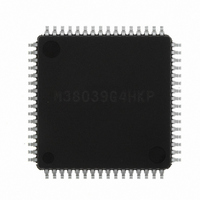
M38039G4HKP#U0 Renesas Electronics America, M38039G4HKP#U0 Datasheet - Page 52

M38039G4HKP#U0
Manufacturer Part Number
M38039G4HKP#U0
Description
IC 3803 MCU ROMLESS 64LQFP
Manufacturer
Renesas Electronics America
Series
740/38000r
Datasheet
1.M38039G4HHPU0.pdf
(105 pages)
Specifications of M38039G4HKP#U0
Core Processor
740
Core Size
8-Bit
Speed
16.8MHz
Connectivity
SIO, UART/USART
Peripherals
LED, PWM, WDT
Number Of I /o
56
Program Memory Size
16KB (16K x 8)
Program Memory Type
QzROM
Ram Size
2K x 8
Voltage - Supply (vcc/vdd)
1.8 V ~ 5.5 V
Data Converters
A/D 16x10b; D/A 2x8b
Oscillator Type
Internal
Operating Temperature
-20°C ~ 85°C
Package / Case
64-LQFP
Lead Free Status / RoHS Status
Lead free / RoHS Compliant
Eeprom Size
-
Available stocks
Company
Part Number
Manufacturer
Quantity
Price
3803 Group (Spec.H QzROM version)
REJ03B0166-0113 Rev.1.13
Page 50 of 100
<Notes concerning serial I/O1>
1. Notes when selecting clock synchronous serial I/O
1.1 Stop of transmission operation
• Note
• Reason
1.2 Stop of receive operation
• Note
1.3 Stop of transmit/receive operation
• Note
• Reason
Clear the serial I/O1 enable bit and the transmit enable bit to
“0” (serial I/O and transmit disabled).
Since transmission is not stopped and the transmission circuit
is not initialized even if only the serial I/O1 enable bit is
cleared to “0” (serial I/O disabled), the internal transmission is
running (in this case, since pins T
S
output). When data is written to the transmit buffer register 1
in this state, data starts to be shifted to the transmit shift
register 1. When the serial I/O1 enable bit is set to “1” at this
time, the data during internally shifting is output to the T
pin and an operation failure occurs.
Clear the receive enable bit to “0” (receive disabled), or clear
the serial I/O1 enable bit to “0” (serial I/O disabled).
Clear both the transmit enable bit and receive enable bit to “0”
(transmit and receive disabled).
(when data is transmitted and received in the clock
synchronous serial I/O mode, any one of data transmission and
reception cannot be stopped.)
In the clock synchronous serial I/O mode, the same clock is
used for transmission and reception. If any one of transmission
and reception is disabled, a bit error occurs because
transmission and reception cannot be synchronized.
In this mode, the clock circuit of the transmission circuit also
operates for data reception. Accordingly, the transmission
circuit does not stop by clearing only the transmit enable bit to
“0” (transmit disabled). Also, the transmission circuit is not
initialized by clearing the serial I/O1 enable bit to “0” (serial
I/O disabled) (refer to 1.1).
RDY1
function as I/O ports, the transmission data is not
Aug 21, 2009
X
D
1
, R
X
D1, S
CLK1
, and
X
D
1
2. Notes when selecting clock asynchronous serial I/O
2.1 Stop of transmission operation
• Note
• Reason
2.2 Stop of receive operation
• Note
2.3 Stop of transmit/receive operation
• Note 1 (only transmission operation is stopped)
• Reason
• Note 2 (only receive operation is stopped)
Clear the transmit enable bit to “0” (transmit disabled). The
transmission operation does not stop by clearing the serial
I/O1 enable bit to “0”.
Since transmission is not stopped and the transmission circuit
is not initialized even if only the serial I/O1 enable bit is
cleared to “0” (serial I/O disabled), the internal transmission is
running (in this case, since pins T
S
output). When data is written to the transmit buffer register 1
in this state, data starts to be shifted to the transmit shift
register 1. When the serial I/O1 enable bit is set to “1” at this
time, the data during internally shifting is output to the T
pin and an operation failure occurs.
Clear the receive enable bit to “0” (receive disabled).
RDY1
RDY1
function as I/O ports, the transmission data is not
function as I/O ports, the transmission data is not
X
X
D
D
1
1
, R
, R
X
X
D
D
1
1
, S
, S
CLK1
CLK1
, and
, and
X
X
D
D
1
1


