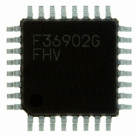
DF36902GFHV Renesas Electronics America, DF36902GFHV Datasheet - Page 432

DF36902GFHV
Manufacturer Part Number
DF36902GFHV
Description
IC H8 MCU FLASH 8K 32QFP
Manufacturer
Renesas Electronics America
Series
H8® H8/300H Tinyr
Specifications of DF36902GFHV
Core Processor
H8/300H
Core Size
16-Bit
Speed
12MHz
Connectivity
SCI
Peripherals
LVD, POR, PWM, WDT
Number Of I /o
18
Program Memory Size
8KB (8K x 8)
Program Memory Type
FLASH
Ram Size
1.5K x 8
Voltage - Supply (vcc/vdd)
3 V ~ 5.5 V
Data Converters
A/D 4x10b
Oscillator Type
Internal
Operating Temperature
-20°C ~ 75°C
Package / Case
32-LQFP
Lead Free Status / RoHS Status
Lead free / RoHS Compliant
Eeprom Size
-
Other names
HD64F36902GFHV
Available stocks
Company
Part Number
Manufacturer
Quantity
Price
Company:
Part Number:
DF36902GFHV
Manufacturer:
Renesas Electronics America
Quantity:
135
Company:
Part Number:
DF36902GFHV
Manufacturer:
Microchip
Quantity:
28
Company:
Part Number:
DF36902GFHV
Manufacturer:
Renesas Electronics America
Quantity:
10 000
- Current page: 432 of 442
- Download datasheet (3Mb)
Rev. 3.00 Sep. 14, 2006 Page 402 of 408
REJ09B0105-0300
Item
5.2.3 RC Trimming Data
Register (RCTRMDR)
5.2.4 Clock Control/Status
Register (CKCSR)
Figure 5.5 Timing Chart of
Switching On-chip Oscillator
Clock to External Clock
Table 5.1 Crystal Resonator
Parameters
Section 7 ROM
Figure 7.1 Flash Memory
Block Configuration
Table 7.3 System Clock
Frequencies for which
Automatic Adjustment of LSI
Bit Rate is Possible
Figure 7.4 Erase/Erase-
Verify Flowchart
Section 8 RAM
Page Revision (See Manual for Details)
73
74
78
82
97
98
105
111
115
Note: * The
The features of the 12-kbyte (including 4 kbytes as the E7 or E8
control program area) flash memory built into the HD64F36912G
and HD64F36902G are summarized below.
Note: * When the E7 or E8 is used, area H'F980 to H'FD7F must
Bit
7
6
5
4
3
2
1
0
Bit
7
6
Programming unit: 64 kbytes
Frequency (MHz) 12
R
Host Bit Rate
9600bps
4800bps
2400bps
S
(Max.)
rising edge of the
clock have elapsed.
not be accessed.
Bit Name Description
TRMD7
TRMD6
TRMD5
TRMD4
TRMD3
TRMD2
TRMD1
TRMD0
Bit Name Description
PMRC1
PMRC0
clock stops to the first
Increment address
halt duration is the duration from the timing when the
8 MHz (on-chip oscillator clock)
8 MHz (on-chip oscillator clock)
8 MHz (on-chip oscillator clock)
System Clock Frequency Range of LSI
Trimming Data
In the flash memory version, the trimming
data is loaded from the flash memory to this
register right after a reset. These bits are
always read as undefined value.
As for the masked ROM version (under
planning), the on-chip oscillator frequency
can be trimmed by rewriting these bits.
Port C Function Select 1 and 0
50
OSC
clock after six clock cycles of the
Verify data = all 1s ?
Read verify data
Yes
No
RC
Related parts for DF36902GFHV
Image
Part Number
Description
Manufacturer
Datasheet
Request
R

Part Number:
Description:
Headers & Wire Housings 20P PLUG METAL COVER
Manufacturer:
Hirose Electric Co Ltd

Part Number:
Description:
Headers & Wire Housings 25P PLUG METAL COVER
Manufacturer:
Hirose Electric Co Ltd

Part Number:
Description:
Headers & Wire Housings 15P PLUG METAL COVER
Manufacturer:
Hirose Electric Co Ltd

Part Number:
Description:
0.4 Mm Pitch, 1.5 Mm Mated Height, Board-to-fine Coaxial Cable Connectors
Manufacturer:
Hirose Electric
Datasheet:

Part Number:
Description:
CONN RECEPT 40POS 0.4MM SMD GOLD
Manufacturer:
Hirose Electric Co Ltd
Datasheet:

Part Number:
Description:
KIT STARTER FOR M16C/29
Manufacturer:
Renesas Electronics America
Datasheet:

Part Number:
Description:
KIT STARTER FOR R8C/2D
Manufacturer:
Renesas Electronics America
Datasheet:

Part Number:
Description:
R0K33062P STARTER KIT
Manufacturer:
Renesas Electronics America
Datasheet:

Part Number:
Description:
KIT STARTER FOR R8C/23 E8A
Manufacturer:
Renesas Electronics America
Datasheet:

Part Number:
Description:
KIT STARTER FOR R8C/25
Manufacturer:
Renesas Electronics America
Datasheet:

Part Number:
Description:
KIT STARTER H8S2456 SHARPE DSPLY
Manufacturer:
Renesas Electronics America
Datasheet:

Part Number:
Description:
KIT STARTER FOR R8C38C
Manufacturer:
Renesas Electronics America
Datasheet:

Part Number:
Description:
KIT STARTER FOR R8C35C
Manufacturer:
Renesas Electronics America
Datasheet:

Part Number:
Description:
KIT STARTER FOR R8CL3AC+LCD APPS
Manufacturer:
Renesas Electronics America
Datasheet:

Part Number:
Description:
KIT STARTER FOR RX610
Manufacturer:
Renesas Electronics America
Datasheet:


