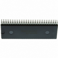
M38039G4HSP#U0 Renesas Electronics America, M38039G4HSP#U0 Datasheet - Page 51

M38039G4HSP#U0
Manufacturer Part Number
M38039G4HSP#U0
Description
IC 740/3803 MCU QZROM 64DIP
Manufacturer
Renesas Electronics America
Series
740/38000r
Datasheet
1.M38039G4HHPU0.pdf
(105 pages)
Specifications of M38039G4HSP#U0
Core Processor
740
Core Size
8-Bit
Speed
16.8MHz
Connectivity
SIO, UART/USART
Peripherals
LED, PWM, WDT
Number Of I /o
56
Program Memory Size
16KB (16K x 8)
Program Memory Type
QzROM
Ram Size
2K x 8
Voltage - Supply (vcc/vdd)
1.8 V ~ 5.5 V
Data Converters
A/D 16x10b; D/A 2x8b
Oscillator Type
Internal
Operating Temperature
-20°C ~ 85°C
Package / Case
64-SDIP (0.750", 19.05mm)
Lead Free Status / RoHS Status
Lead free / RoHS Compliant
Eeprom Size
-
3803 Group (Spec.H QzROM version)
REJ03B0166-0113 Rev.1.13
Page 49 of 100
Fig 40. Structure of serial I/O1 control registers
b7
b7
b0
b0
UART1 control register
(UART1CON : address 001B
Serial I/O1 status register
(SIO1STS : address 0019
Transmit buffer empty flag (TBE)
Receive buffer full flag (RBF)
Transmit shift completion flag (TSC)
Overrun error flag (OE)
Parity error flag (PE)
Framing error flag (FE)
Summing error flag (SE)
Not used (returns “1” when read)
Character length selection bit (CHAS)
Parity enable bit (PARE)
Parity selection bit (PARS)
Stop bit length selection bit (STPS)
P4
Not used (return “1” when read)
0: Buffer full
1: Buffer empty
0: Buffer empty
1: Buffer full
0: Transmit shift in progress
1: Transmit shift completed
0: No error
1: Overrun error
0: No error
1: Parity error
0: No error
1: Framing error
0: (OE) U (PE) U (FE)=0
1: (OE) U (PE) U (FE)=1
0: 8 bits
1: 7 bits
0: Parity checking disabled
1: Parity checking enabled
0: Even parity
1: Odd parity
0: 1 stop bit
1: 2 stop bits
0: CMOS output (in output mode)
1: N-channel open drain output (in output mode)
5
/T
X
D
1
P-channel output disable bit (POFF)
Aug 21, 2009
16
)
16
)
b7
b0
Serial I/O1 control register
(SIO1CON : address 001A
BRG count source selection bit (CSS)
Serial I/O1 synchronous clock selection bit (SCS)
S
Transmit interrupt source selection bit (TIC)
Transmit enable bit (TE)
Receive enable bit (RE)
Serial I/O1 mode selection bit (SIOM)
Serial I/O1 enable bit (SIOE)
0: f(X
1: f(X
0: BRG output divided by 4 when clock synchronous
1: External clock input when clock synchronous serial
0: P4
1: P4
0: Interrupt when transmit buffer has emptied
1: Interrupt when transmit shift operation is completed
0: Transmit disabled
1: Transmit enabled
0: Receive disabled
1: Receive enabled
0: Clock asynchronous (UART) serial I/O
1: Clock synchronous serial I/O
0: Serial I/O1 disabled
1: Serial I/O1 enabled
RDY1
serial I/O1 is selected, BRG output divided by 16
when UART is selected.
I/O1 is selected, external clock input divided by 16
when UART is selected.
(pins P4
(pins P4
7
7
IN
IN
output enable bit (SRDY)
pin operates as normal I/O pin
pin operates as S
) (f(X
)/4 (f(X
4
4
CIN
to P4
to P4
CIN
) in low-speed mode)
)/4 in low-speed mode)
7
7
operate as normal I/O pins)
operate as serial I/O1 pins)
16
RDY1
)
output pin


