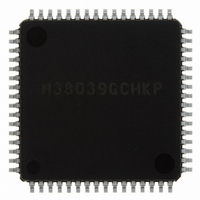
M38039GCHKP#U0 Renesas Electronics America, M38039GCHKP#U0 Datasheet - Page 66

M38039GCHKP#U0
Manufacturer Part Number
M38039GCHKP#U0
Description
IC 740/3803 MCU QZROM 64LQFP
Manufacturer
Renesas Electronics America
Series
740/38000r
Datasheet
1.M38039G4HHPU0.pdf
(105 pages)
Specifications of M38039GCHKP#U0
Core Processor
740
Core Size
8-Bit
Speed
16.8MHz
Connectivity
SIO, UART/USART
Peripherals
LED, PWM, WDT
Number Of I /o
56
Program Memory Size
48KB (48K x 8)
Program Memory Type
QzROM
Ram Size
2K x 8
Voltage - Supply (vcc/vdd)
1.8 V ~ 5.5 V
Data Converters
A/D 16x10b; D/A 2x8b
Oscillator Type
Internal
Operating Temperature
-20°C ~ 85°C
Package / Case
64-LQFP
Lead Free Status / RoHS Status
Lead free / RoHS Compliant
Eeprom Size
-
Available stocks
Company
Part Number
Manufacturer
Quantity
Price
3803 Group (Spec.H QzROM version)
REJ03B0166-0113 Rev.1.13
Page 64 of 100
D/A CONVERTER
The 3803 group (Spec.H QzROM version) has two internal D/A
converters (DA
The D/A conversion is performed by setting the value in each
DAi conversion register (i = 1 or 2). The result of D/A
conversion is output from the DA
output enable bit (i = 1 or 2) to “1”.
When using the D/A converter, the corresponding port direction
register bit (P3
status).
The output analog voltage V is determined by the value n
(decimal notation) in the DAi conversion register (i = 1 or 2) as
follows:
V = V
At reset, the DAi conversion register (i = 1 or 2) is cleared to
“00
“0”, and the P3
impedance.
The DA output does not have buffers. Accordingly, connect an
external buffer when driving a low-impedance load.
Fig 58. Equivalent connection circuit of D/A converter (DA1)
16
Where V
DA
”, and the DAi output enable bit (i = 1 or 2) is cleared to
REF
1
conversion register
× n/256 (n = 0 to 255)
P3
0
REF
/DA
1
0
and DA
/DA
is the reference voltage.
1
0
A
V
/DA
VSS
REF
1
“1”
or P3
2
1
“0”
) with 8-bit resolution.
and P3
DA
1
/DA
MSB
1
1
output enable bit
“0”
or DA
2
1
) must be set to “0” (input
/DA
Aug 21, 2009
2
2
“1”
pin by setting the DAi
2R
pins become high
R
2R
R
2R
R
Fig 57. Block diagram of D/A converter
2R
R
R-2R resistor ladder
R-2R resistor ladder
DA
DA
1
2
conversion register (8)
conversion register (8)
2R
R
2R
R
DA
DA
1
2
output enable bit
output enable bit
2R
R
LSB
2R
2R
P3
P3
0
1
/DA
/DA
1
2


