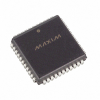
DS89C450-QNL+ Maxim Integrated Products, DS89C450-QNL+ Datasheet - Page 13

DS89C450-QNL+
Manufacturer Part Number
DS89C450-QNL+
Description
IC MCU FLASH 64KB 33MHZ 44-PLCC
Manufacturer
Maxim Integrated Products
Series
89Cr
Datasheet
1.DS89C450-KIT.pdf
(46 pages)
Specifications of DS89C450-QNL+
Core Processor
8051
Core Size
8-Bit
Speed
33MHz
Connectivity
EBI/EMI, SIO, UART/USART
Peripherals
Power-Fail Reset, WDT
Number Of I /o
32
Program Memory Size
64KB (64K x 8)
Program Memory Type
FLASH
Ram Size
1K x 8
Voltage - Supply (vcc/vdd)
4.5 V ~ 5.5 V
Oscillator Type
External
Operating Temperature
-40°C ~ 85°C
Package / Case
44-LCC, 44-PLCC
Processor Series
89C
Core
8051
Data Bus Width
8 bit
Data Ram Size
1 KB
Maximum Clock Frequency
33 MHz
Number Of Programmable I/os
32
Number Of Timers
3
Operating Supply Voltage
5 V
Maximum Operating Temperature
+ 85 C
Mounting Style
SMD/SMT
3rd Party Development Tools
PK51, CA51, A51, ULINK2
Development Tools By Supplier
DS89C450-K00
Minimum Operating Temperature
- 40 C
Interface Type
UART
Lead Free Status / RoHS Status
Lead free / RoHS Compliant
Eeprom Size
-
Data Converters
-
Lead Free Status / Rohs Status
Lead free / RoHS Compliant
PIN DESCRIPTION (continued)
PDIP
21
22
23
24
25
26
27
28
10
11
12
13
14
15
16
17
31
1
2
3
4
5
6
7
8
PLCC
24
25
26
27
28
29
30
31
11
13
14
15
16
17
18
19
35
2
3
4
5
6
7
8
9
PIN
TQFP
40
41
42
43
44
18
19
20
21
22
23
24
25
10
11
12
13
29
1
2
3
5
7
8
9
P2.2 (A10)
P2.3 (A11)
P2.4 (A12)
P2.5 (A13)
P2.6 (A14)
P2.7 (A15)
P2.0 (A8)
P2.1 (A9)
NAME
P1.0
P1.1
P1.2
P1.3
P1.4
P1.5
P1.6
P1.7
P3.0
P3.1
P3.2
P3.3
P3.4
P3.5
P3.6
P3.7
EA
Port 2 (A8–A15), I/O. Port 2 is an 8-bit, bidirectional I/O port. The reset condition of port 2
is logic high. In this state, a weak pullup holds the port high. This condition also serves as
an input mode, since any external circuit that writes to the port overcomes the weak
pullup. When software writes a 0 to any port pin, the DS89C430/DS89C450 activate a
strong pulldown that remains on until either a 1 is written or a reset occurs. Writing a 1
after the port has been at 0 causes a strong transition driver to turn on, followed by a
weaker sustaining pullup. Once the momentary strong driver turns off, the port again
becomes both the output high and input state. As an alternate function, port 2 can function
as the MSB of the external address bus when reading external program memory and
read/write external RAM or peripherals. In page mode 1, port 2 provides both the MSB and
LSB of the external address bus. In page mode 2, it provides the MSB and data.
Port 3, I/O. Port 3 functions as both an 8-bit, bidirectional I/O port and an alternate
functional interface for external interrupts, serial port 0, timer 0 and 1 inputs, and RD and
WR strobes. The reset condition of port 3 is with all bits at a logic 1. In this state, a weak
pullup holds the port high. This condition also serves as an input mode, since any external
circuit that writes to the port overcomes the weak pullup. When software writes a 0 to any
port pin, the DS89C430/DS89C450 activate a strong pulldown that remains on until either
a 1 is written or a reset occurs. Writing a 1 after the port has been at 0 causes a strong
transition driver to turn on, followed by a weaker sustaining pullup. Once the momentary
strong driver turns off, the port again becomes both the output high and input state. The
alternate modes of port 3 are as follows:
External Access. Allows selection of internal or external program memory. Connect to
ground to force the DS89C430/DS89C450 to use an external memory program memory.
The internal RAM is still accessible as determined by register settings. Connect to V
use internal flash memory.
Port 1, I/O. Port 1 functions as both an 8-bit, bidirectional I/O port and an alternate
functional interface for timer 2 I/O, new external interrupts, and new serial port 1. The
reset condition of port 1 is with all bits at logic 1. In this state, a weak pullup holds the port
high. This condition also serves as an input state, since any external circuit that writes to
the port overcomes the weak pullup. When software writes a 0 to any port pin, the
DS89C430/DS89C450 activate a strong pulldown that remains on until either a 1 is
written or a reset occurs. Writing a 1 after the port has been at 0 causes a strong
transition driver to turn on, followed by a weaker sustaining pullup. Once the momentary
strong driver turns off, the port again becomes the output high (and input) state. The
alternate functions of port 1 are as follows:
PORT
P3.0
P3.1
P3.2
P3.3
P3.4
P3.5
P3.6
P3.7
PORT
P1.0
P1.1
P1.2
P1.3
P1.4
P1.5
P1.6
P1.7
DS89C430/DS89C450 Ultra-High-Speed Flash Microcontrollers
13 of 46
INT5
ALTERNATE
T2
T2EX
RXD1
TXD1
INT2
INT3
INT4
ALTERNATE
RXD0
TXD0
INT0
INT1
T0
T1
WR
RD
FUNCTION
External I/O for Timer/Counter2
Timer 2 Capture/Reload Trigger
Serial Port 1 Receive
Serial Port 1 Transmit
External Interrupt 2 (Positive Edge Detect)
External Interrupt 3 (Negative Edge Detect)
External Interrupt 4 (Positive Edge Detect)
External Interrupt 5 (Negative Edge Detect)
FUNCTION
Serial Port 0 Receive
Serial Port 0 Transmit
External Interrupt 0
External Interrupt 1
Timer 0 External Input
Timer 1 External Input
External Data Memory Write Strobe
External Data Memory Read Strobe
FUNCTION
CC
to


