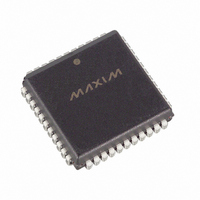
DS89C450-QNL+ Maxim Integrated Products, DS89C450-QNL+ Datasheet - Page 39

DS89C450-QNL+
Manufacturer Part Number
DS89C450-QNL+
Description
IC MCU FLASH 64KB 33MHZ 44-PLCC
Manufacturer
Maxim Integrated Products
Series
89Cr
Datasheet
1.DS89C450-KIT.pdf
(46 pages)
Specifications of DS89C450-QNL+
Core Processor
8051
Core Size
8-Bit
Speed
33MHz
Connectivity
EBI/EMI, SIO, UART/USART
Peripherals
Power-Fail Reset, WDT
Number Of I /o
32
Program Memory Size
64KB (64K x 8)
Program Memory Type
FLASH
Ram Size
1K x 8
Voltage - Supply (vcc/vdd)
4.5 V ~ 5.5 V
Oscillator Type
External
Operating Temperature
-40°C ~ 85°C
Package / Case
44-LCC, 44-PLCC
Processor Series
89C
Core
8051
Data Bus Width
8 bit
Data Ram Size
1 KB
Maximum Clock Frequency
33 MHz
Number Of Programmable I/os
32
Number Of Timers
3
Operating Supply Voltage
5 V
Maximum Operating Temperature
+ 85 C
Mounting Style
SMD/SMT
3rd Party Development Tools
PK51, CA51, A51, ULINK2
Development Tools By Supplier
DS89C450-K00
Minimum Operating Temperature
- 40 C
Interface Type
UART
Lead Free Status / RoHS Status
Lead free / RoHS Compliant
Eeprom Size
-
Data Converters
-
Lead Free Status / Rohs Status
Lead free / RoHS Compliant
Figure 14. System Clock Sources
Bandgap-Monitored Interrupt and Reset Generation
The power monitor in the DS89C430 monitors the V
Whenever V
(WDCON.5) is set, causing the device to vector to address 33h. The power-fail interrupt status bit PFI (WDCON.4)
is set any time V
below V
power-on reset timeout before starting program execution. When V
processor is held in reset until V
is within tolerance and the clock source has had time to stabilize. Once the reset timeout period has elapsed, the
reset condition is removed automatically and software execution begins at the reset vector location of 0000h. The
power-on reset flag POR (WDCON.6) is set to logic 1 to indicate a power-on reset has occurred, and can only be
cleared by software.
When the DS89C430 enters stop mode, the bandgap, reset comparator, and power-fail interrupt comparator are
automatically disabled to conserve power if the BGS (EXIF.0) bit is set to logic 0. This is the lowest power mode. If
BGS is set to logic 1, the bandgap reference, reset comparator, and the power-fail comparator are powered up,
although in a mode that reduces their power consumption.
OSCILLATOR
RST
CRYSTAL
, a reset is issued internally to halt program execution. Following power-up, a power-on reset initiates a
CC
falls below V
CC
transitions below V
PFW
ENABLE
RING
, an interrupt is generated if the corresponding power-fail interrupt-enable bit EPFI
CC
4X/2X
CTM
> V
RST
PFW
and a delay of 65,536 oscillator cycles has elapsed, to ensure that power
, and can only be cleared by software once set. Similarly, as V
MULTIPLIER
DIVIDE 1024
OSCILLATOR
CLOCK
DS89C430/DS89C450 Ultra-High-Speed Flash Microcontrollers
RING
39 of 46
CC
pin in relation to the on-chip bandgap voltage reference.
CD0
CD1
CC
is first applied to the DS89C430, the
SELECTOR
MUX
SYSTEM
CLOCK
CC
falls


