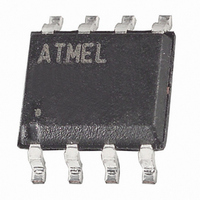
AT90LS2323-4SI Atmel, AT90LS2323-4SI Datasheet - Page 44

AT90LS2323-4SI
Manufacturer Part Number
AT90LS2323-4SI
Description
IC MCU 2K FLASH 4MHZ LV 8-SOIC
Manufacturer
Atmel
Series
AVR® 90LSr
Datasheet
1.AT90LS2323-4PC.pdf
(64 pages)
Specifications of AT90LS2323-4SI
Core Processor
AVR
Core Size
8-Bit
Speed
4MHz
Connectivity
SPI
Peripherals
Brown-out Detect/Reset, POR, WDT
Number Of I /o
3
Program Memory Size
2KB (1K x 16)
Program Memory Type
FLASH
Eeprom Size
128 x 8
Ram Size
128 x 8
Voltage - Supply (vcc/vdd)
2.7 V ~ 6 V
Oscillator Type
Internal
Operating Temperature
-40°C ~ 85°C
Package / Case
8-SOIC (5.3mm Width), 8-SOP, 8-SOEIAJ
Lead Free Status / RoHS Status
Contains lead / RoHS non-compliant
Data Converters
-
Available stocks
Company
Part Number
Manufacturer
Quantity
Price
Part Number:
AT90LS2323-4SI
Manufacturer:
ATMEL/爱特梅尔
Quantity:
20 000
Data Polling EEPROM
Data Polling Flash
44
AT90S/LS2323/2343
7. At the end of the programming session, RESET can be set high to commence
8. Power-off sequence (if needed):
When a byte is being programmed into the EEPROM, reading the address location
being programmed will give the value P1 until the auto-erase is finished, and then the
value P2 will be given. See Table 18 for P1 and P2 values.
At the time the device is ready for a new EEPROM byte, the programmed value will read
correctly. This is used to determine when the next byte can be written. This will not work
for the values P1 and P2, so when programming these values, the user will have to wait
for at least the prescribed time t
for t
of addresses that are meant to contain $FF can be skipped. This does not apply if the
EEPROM is reprogrammed without first chip-erasing the device.
Table 18. Read Back Value during EEPROM Polling
When a byte is being programmed into the Flash, reading the address location being
programmed will give the value $FF. At the time the device is ready for a new byte, the
programmed value will read correctly. This is used to determine when the next byte can
be written. This will not work for the value $FF, so when programming this value, the
user will have to wait for at least t
erased device contains $FF in all locations, programming of addresses that are meant
to contain $FF can be skipped.
Figure 36. Low-voltage Serial Downloading Waveforms
Part
AT90S2323
AT90S2343
SERIAL DATA OUTPUT
SERIAL CLOCK INPUT
Set CLOCK/XTAL1 to “0”.
Set RESET to “1”.
Turn V
WD_PROG
normal operation.
SERIAL DATA INPUT
CC
value. As a chip-erased device contains $FF in all locations, programming
PB0(MOSI)
PB1(MISO)
PB2(SCK)
power off.
MSB
MSB
WD_PROG
WD_PROG
before programming the next byte. See Table 22
before programming the next byte. As a chip-
P1
$00
$00
P2
$FF
$FF
LSB
LSB
1004D–09/01


