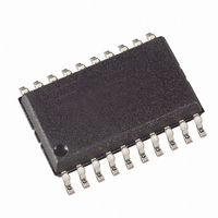
AT90S2313-4SI Atmel, AT90S2313-4SI Datasheet - Page 32

AT90S2313-4SI
Manufacturer Part Number
AT90S2313-4SI
Description
MCU 2K FLASH 4MHZ 20-SOIC
Manufacturer
Atmel
Series
AVR® 90Sr
Datasheet
1.AT90S2313-10PC.pdf
(92 pages)
Specifications of AT90S2313-4SI
Core Processor
AVR
Core Size
8-Bit
Speed
4MHz
Connectivity
SPI, UART/USART
Peripherals
Brown-out Detect/Reset, POR, PWM, WDT
Number Of I /o
15
Program Memory Size
2KB (1K x 16)
Program Memory Type
FLASH
Eeprom Size
128 x 8
Ram Size
128 x 8
Voltage - Supply (vcc/vdd)
2.7 V ~ 6 V
Oscillator Type
External
Operating Temperature
-40°C ~ 85°C
Package / Case
20-SOIC (7.5mm Width)
Data Bus Width
8 bit
Data Ram Size
128 B
Interface Type
SPI, UART
Maximum Clock Frequency
4 MHz
Number Of Programmable I/os
15
Number Of Timers
1 x 8 bit
Operating Supply Voltage
2.7 V to 6 V
Maximum Operating Temperature
+ 85 C
Mounting Style
SMD/SMT
Minimum Operating Temperature
- 40 C
Lead Free Status / RoHS Status
Contains lead / RoHS non-compliant
Data Converters
-
Lead Free Status / Rohs Status
No
Available stocks
Company
Part Number
Manufacturer
Quantity
Price
Part Number:
AT90S2313-4SI
Manufacturer:
ATMEL/爱特梅尔
Quantity:
20 000
Timer/Counter1 Control
Register B – TCCR1B
32
AT90S2313
• Bits 1, 0 – PWM11, PWM10: Pulse Width Modulator Select Bits
These bits select PWM operation of Timer/Counter1 as specified in Table 9. This mode
is described on page 35.
Table 9. PWM Mode Select
• Bit 7 – ICNC1: Input Capture1 Noise Canceler (4 CKs)
When the ICNC1 bit is cleared (zero), the input capture trigger noise canceler function is
disabled. The input capture is triggered at the first rising/falling edge sampled on the ICP
(input capture pin) as specified. When the ICNC1 bit is set (one), four successive sam-
ples are measured on the ICP (input capture pin), and all samples must be high/low
according to the input capture trigger specification in the ICES1 bit. The actual sampling
frequency is the XTAL clock frequency.
• Bit 6 – ICES1: Input Capture1 Edge Select
While the ICES1 bit is cleared (zero), the Timer/Counter1 contents are transferred to the
Input Capture Register (ICR1) on the falling edge of the input capture pin (ICP). While
the ICES1 bit is set (one), the Timer/Counter1 contents are transferred to the Input Cap-
ture Register (ICR1) on the rising edge of the input capture pin (ICP).
• Bits 5, 4 – Res: Reserved Bits
These bits are reserved bits in the AT90S2313 and always read zero.
• Bit 3 – CTC1: Clear Timer/Counter1 on Compare Match
When the CTC1 control bit is set (one), the Timer/Counter1 is reset to $0000 in the clock
cycle after a compareA match. If the CTC1 control bit is cleared, Timer/Counter1 contin-
ues counting and is unaffected by a compare match. Since the compare match is
detected in the CPU clock cycle following the match, this function will behave differently
when a prescaling higher than 1 is used for the timer. When a prescaling of 1 is used,
and the Compare A Register is set to C, the timer will count as follows if CTC1 is set:
... | C-2 | C-1 | C | 0 | 1 |...
When the prescaler is set to divide by 8, the timer will count like this:
... | C-2, C-2, C-2, C-2, C-2, C-2, C-2, C-2 | C-1, C-1, C-1, C-1, C-1, C-1, C-1, C-1 | C, 0,
0, 0, 0, 0, 0, 0 |...
In PWM mode, this bit has no effect.
Bit
$2E ($4E)
Read/Write
Initial value
PWM11
0
0
1
1
ICNC1
R/W
7
0
PWM10
0
1
0
1
ICES1
R/W
6
0
Description
PWM operation of Timer/Counter1 is disabled
Timer/Counter1 is an 8-bit PWM
Timer/Counter1 is a 9-bit PWM
Timer/Counter1 is a 10-bit PWM
R
5
–
0
R
4
–
0
CTC1
R/W
3
0
CS12
R/W
2
0
CS11
R/W
1
0
CS10
R/W
0
0
0839I–AVR–06/02
TCCR1B


