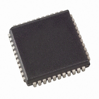
AT90S8515-8JC Atmel, AT90S8515-8JC Datasheet - Page 81

AT90S8515-8JC
Manufacturer Part Number
AT90S8515-8JC
Description
IC MCU 8K FLSH 8MHZ 44PLCC
Manufacturer
Atmel
Series
AVR® 90Sr
Datasheets
1.AT90S8515-4AC.pdf
(112 pages)
2.AT90S8515-4AC.pdf
(4 pages)
3.AT90S8515-4AC.pdf
(4 pages)
Specifications of AT90S8515-8JC
Core Processor
AVR
Core Size
8-Bit
Speed
8MHz
Connectivity
SPI, UART/USART
Peripherals
Brown-out Detect/Reset, POR, PWM, WDT
Number Of I /o
32
Program Memory Size
8KB (4K x 16)
Program Memory Type
FLASH
Eeprom Size
512 x 8
Ram Size
512 x 8
Voltage - Supply (vcc/vdd)
4 V ~ 6 V
Oscillator Type
Internal
Operating Temperature
0°C ~ 70°C
Package / Case
44-PLCC
Lead Free Status / RoHS Status
Contains lead / RoHS non-compliant
Data Converters
-
Available stocks
Company
Part Number
Manufacturer
Quantity
Price
Company:
Part Number:
AT90S8515-8JC
Manufacturer:
ATM
Quantity:
3 670
Company:
Part Number:
AT90S8515-8JC
Manufacturer:
ATM
Quantity:
3 670
Company:
Part Number:
AT90S8515-8JC
Manufacturer:
ATMEL
Quantity:
5 510
Chip Erase
Programming the Flash
0841G–09/01
The Chip Erase command will erase the Flash and EEPROM memories and the Lock
bits. The Lock bits are not reset until the Flash and EEPROM have been completely
erased. The Fuse bits are not changed. Chip Erase must be performed before the Flash
or EEPROM is reprogrammed.
Load Command “Chip Erase”
1. Set XA1, XA0 to “10”. This enables command loading.
2. Set BS to “0”.
3. Set DATA to “1000 0000”. This is the command for Chip Erase.
4. Give XTAL1 a positive pulse. This loads the command.
5. Give WR a t
A: Load Command “Write Flash”
1. Set XA1, XA0 to “10”. This enables command loading.
2. Set BS to “0”.
3. Set DATA to “0001 0000”. This is the command for Write Flash.
4. Give XTAL1 a positive pulse. This loads the command.
B: Load Address High Byte
1. Set XA1, XA0 to “00”. This enables address loading.
2. Set BS to “1”. This selects high byte.
3. Set DATA = Address high byte ($00 - $0F).
4. Give XTAL1 a positive pulse. This loads the address high byte.
C: Load Address Low Byte
1. Set XA1, XA0 to “00”. This enables address loading.
2. Set BS to “0”. This selects low byte.
3. Set DATA = Address low byte ($00 - $FF).
4. Give XTAL1 a positive pulse. This loads the address low byte.
D: Load Data Low Byte
1. Set XA1, XA0 to “01”. This enables data loading.
2. Set DATA = Data low byte ($00 - $FF).
3. Give XTAL1 a positive pulse. This loads the data low byte.
E: Write Data Low Byte
1. Set BS to “0”. This selects low data.
2. Give WR a negative pulse. This starts programming of the data byte. RDY/BSY
3. Wait until RDY/BSY goes high to program the next byte.
(See Figure 61 for signal waveforms.)
F: Load Data High Byte
1. Set XA1, XA0 to “01”. This enables data loading.
2. Set DATA = Data high byte ($00 - $FF).
3. Give XTAL1 a positive pulse. This loads the data high byte.
G: Write Data High Byte
on page 85 for t
RDY/BSY pin.
goes low.
WLWH_CE
WLWH_CE
-wide negative pulse to execute Chip Erase. See Table 30
value. Chip Erase does not generate any activity on the
AT90S8515
81


