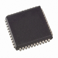
AT90S8515A-8JC Atmel, AT90S8515A-8JC Datasheet - Page 12

AT90S8515A-8JC
Manufacturer Part Number
AT90S8515A-8JC
Description
IC MCU 8K FLSH 8MHZ 44PLCC
Manufacturer
Atmel
Series
AVR® 90Sr
Datasheets
1.AT90S8515-4AC.pdf
(112 pages)
2.AT90S8515-4AC.pdf
(4 pages)
3.AT90S8515-4AC.pdf
(4 pages)
Specifications of AT90S8515A-8JC
Core Processor
AVR
Core Size
8-Bit
Speed
8MHz
Connectivity
SPI, UART/USART
Peripherals
Brown-out Detect/Reset, POR, PWM, WDT
Number Of I /o
32
Program Memory Size
8KB (4K x 16)
Program Memory Type
FLASH
Eeprom Size
512 x 8
Ram Size
512 x 8
Voltage - Supply (vcc/vdd)
4 V ~ 6 V
Oscillator Type
Internal
Operating Temperature
0°C ~ 70°C
Package / Case
44-PLCC
Lead Free Status / RoHS Status
Contains lead / RoHS non-compliant
Data Converters
-
SRAM Data Memory –
Internal and External
12
AT90S8515
Figure 8 shows how the AT90S8515 SRAM memory is organized.
Figure 8. SRAM Organization
The lower 608 data memory locations address the Register file, the I/O memory and the
internal data SRAM. The first 96 locations address the Register file + I/O memory, and
the next 512 locations address the internal data SRAM. An optional external data SRAM
can be placed in the same SRAM memory space. This SRAM will occupy the location
following the internal SRAM and up to as much as 64K - 1, depending on SRAM size.
When the addresses accessing the data memory space exceed the internal data SRAM
locations, the external data SRAM is accessed using the same instructions as for the
internal data SRAM access. When the internal data space is accessed, the read and
write strobe pins (RD and WR) are inactive during the whole access cycle. External
SRAM operation is enabled by setting the SRE bit in the MCUCR register. See page 29
for details.
Accessing external SRAM takes one additional clock cycle per byte compared to access
of the internal SRAM. This means that the commands LD, ST, LDS, STS, PUSH and
POP take one additional clock cycle. If the stack is placed in external SRAM, interrupts,
subroutine calls and returns take two clock cycles extra because the 2-byte program
counter is pushed and popped. When external SRAM interface is used with wait state,
I/O Registers
Register File
R29
R30
R31
$3D
$3E
$00
$01
$02
$3F
R0
R1
R2
…
…
Data Address Space
External SRAM
Internal SRAM
$FFFE
$001D
$001E
$001F
$005D
$005E
$005F
$025E
$025F
$FFFF
$0000
$0001
$0002
$0020
$0021
$0022
$0060
$0061
$0260
$0261
…
…
…
…
0841G–09/01


