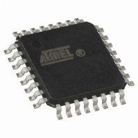
AT90LS4433-4AC Atmel, AT90LS4433-4AC Datasheet - Page 74

AT90LS4433-4AC
Manufacturer Part Number
AT90LS4433-4AC
Description
IC MCU 4K 4MHZ A/D LV 32TQFP
Manufacturer
Atmel
Series
AVR® 90LSr
Datasheet
1.AT90S4433-8AC.pdf
(126 pages)
Specifications of AT90LS4433-4AC
Core Processor
AVR
Core Size
8-Bit
Speed
4MHz
Connectivity
SPI, UART/USART
Peripherals
Brown-out Detect/Reset, POR, PWM, WDT
Number Of I /o
20
Program Memory Size
4KB (2K x 16)
Program Memory Type
FLASH
Eeprom Size
256 x 8
Ram Size
128 x 8
Voltage - Supply (vcc/vdd)
2.7 V ~ 6 V
Data Converters
A/D 6x10b
Oscillator Type
External
Operating Temperature
0°C ~ 70°C
Package / Case
32-TQFP, 32-VQFP
Lead Free Status / RoHS Status
Contains lead / RoHS non-compliant
Available stocks
Company
Part Number
Manufacturer
Quantity
Price
Company:
Part Number:
AT90LS4433-4AC
Manufacturer:
ATM
Quantity:
72
- Current page: 74 of 126
- Download datasheet (2Mb)
74
AT90S/LS4433
controlled by DDB2. When the pin is forced to be an input, the pull-up can still be con-
trolled by the PORTB2 bit. See the description of the SPI port for further details.
• OC1 – Port B, Bit 1
OC1, Output Compare Match output: PB1 pin can serve as an external output for the
Timer/Counter1 Output Compare. The pin has to be configured as an output (DDB1 set
[one]) to serve this function. See the timer description on how to enable this function.
The OC1 pin is also the output pin for the PWM mode timer function.
• ICP – Port B, Bit 0
ICP, Input Capture Pin: PB0 pin can serve as an external input for the Timer/Counter1
input capture. The pin has to be configured as an input (DDB0 cleared [zero]) to serve
this function. See the timer description on how to enable this function.
Figure 50. Port B Schematic Diagram (Pin PB0)
PB0
WP:
WD:
RL:
RP:
RD:
ACIC:
ACO:
MOS
PULL-
UP
WRITE PORTB
WRITE DDRB
READ PORTB LATCH
READ PORTB PIN
READ DDRB
COMPARATOR IC ENABLE
COMPARATOR OUTPUT
0
1
NOISE CANCELER
ICNC1
RL
RP
EDGE SELECT
Q
Q
ICES1
PORTB0
RESET
RESET
DDB6
WD
WP
RD
R
C
R
C
D
D
ICF1
ACIC
ACO
1042H–AVR–04/03
Related parts for AT90LS4433-4AC
Image
Part Number
Description
Manufacturer
Datasheet
Request
R

Part Number:
Description:
DEV KIT FOR AVR/AVR32
Manufacturer:
Atmel
Datasheet:

Part Number:
Description:
INTERVAL AND WIPE/WASH WIPER CONTROL IC WITH DELAY
Manufacturer:
ATMEL Corporation
Datasheet:

Part Number:
Description:
Low-Voltage Voice-Switched IC for Hands-Free Operation
Manufacturer:
ATMEL Corporation
Datasheet:

Part Number:
Description:
MONOLITHIC INTEGRATED FEATUREPHONE CIRCUIT
Manufacturer:
ATMEL Corporation
Datasheet:

Part Number:
Description:
AM-FM Receiver IC U4255BM-M
Manufacturer:
ATMEL Corporation
Datasheet:

Part Number:
Description:
Monolithic Integrated Feature Phone Circuit
Manufacturer:
ATMEL Corporation
Datasheet:

Part Number:
Description:
Multistandard Video-IF and Quasi Parallel Sound Processing
Manufacturer:
ATMEL Corporation
Datasheet:

Part Number:
Description:
High-performance EE PLD
Manufacturer:
ATMEL Corporation
Datasheet:

Part Number:
Description:
8-bit Flash Microcontroller
Manufacturer:
ATMEL Corporation
Datasheet:

Part Number:
Description:
2-Wire Serial EEPROM
Manufacturer:
ATMEL Corporation
Datasheet:


