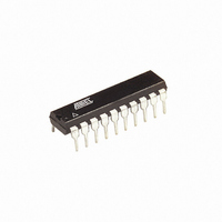
ATTINY26-16PI Atmel, ATTINY26-16PI Datasheet - Page 52

ATTINY26-16PI
Manufacturer Part Number
ATTINY26-16PI
Description
IC AVR MCU 2K 16MHZ IND 20-DIP
Manufacturer
Atmel
Series
AVR® ATtinyr
Specifications of ATTINY26-16PI
Core Processor
AVR
Core Size
8-Bit
Speed
16MHz
Connectivity
USI
Peripherals
Brown-out Detect/Reset, POR, PWM, WDT
Number Of I /o
16
Program Memory Size
2KB (1K x 16)
Program Memory Type
FLASH
Eeprom Size
128 x 8
Ram Size
128 x 8
Voltage - Supply (vcc/vdd)
4.5 V ~ 5.5 V
Data Converters
A/D 11x10b
Oscillator Type
Internal
Operating Temperature
-40°C ~ 85°C
Package / Case
20-DIP (0.300", 7.62mm)
Lead Free Status / RoHS Status
Contains lead / RoHS non-compliant
- Current page: 52 of 182
- Download datasheet (3Mb)
The masking alternate function is the pin usage as RESET. Digital input is enabled on pin PB7
also in SLEEP modes, if the pin change interrupt is enabled and not masked by the alternate
function.
• ADC9/INT0/T0/PCINT1 – Port B, Bit 6
ADC9: ADC Input Channel 9. Configure the port pins as inputs with the internal pull-ups
switched off to avoid the digital port function from interfering with the function of the analog to
digital converter.
INT0: External Interrupt source 0: The PB6 pin can serve as an external interrupt source
enabled by setting (one) the bit INT0 in the General Input Mask Register (GIMSK).
T0: Timer/Counter0 External Counter Clock input is enabled by setting (one) the bits CS02 and
CS01 in the Timer/Counter0 Control Register (TCCR0).
PCINT1: Pin Change Interrupt 1 pin. Pin change interrupt is enabled on pin when global interrupt
is enabled, pin change interrupt is enabled and the alternate functions do not mask the interrupt.
The masking alternate functions are the external low level Interrupt source 0 (INT0) and the
Timer/Counter0 External Counter clock input (T0). Digital input is enabled on pin PB6 also in
SLEEP modes, if the pin change interrupt is enabled and not masked by the alternate functions.
• ADC8/XTAL2/PCINT1 – Port B, Bit 5
ADC8: ADC Input Channel 8. Configure the port pins as inputs with the internal pull-ups
switched off to avoid the digital port function from interfering with the function of the analog to
digital converter.
XTAL2: Chip Clock Oscillator pin 2. Used as clock pin for all chip clock sources except internal
calibrateble RC Oscillator, external clock and PLL clock. When used as a clock pin, the pin can
not be used as an I/O pin. When using internal calibratable RC Oscillator, External clock or PLL
clock as Chip clock sources, PB5 serves as an ordinary I/O pin.
PCINT1: Pin Change Interrupt 1 pin. Pin change interrupt is enabled on pin when global interrupt
is enabled, pin change interrupt is enabled and the alternate functions do not mask the interrupt.
The masking alternate functions are the XTAL2 outputs. Digital input is enabled on pin PB5 also
in SLEEP modes, if the pin change interrupt is enabled and not masked by the alternate
functions.
• ADC7/XTAL1/PCINT1 – Port B, Bit 4
ADC7: ADC Input Channel 7. Configure the port pins as inputs with the internal pull-ups
switched off to avoid the digital port function from interfering with the function of the analog to
digital converter.
XTAL1: Chip Clock Oscillator pin 1. Used for all chip clock sources except internal calibrateble
RC oscillator and PLL clock. When used as a clock pin, the pin can not be used as an I/O pin.
When using internal calibratable RC Oscillator or PLL clock as chip clock sources, PB4 serves
as an ordinary I/O pin.
PCINT1: Pin Change Interrupt 1 pin. Pin change interrupt is enabled on pin when global interrupt
is enabled, pin change interrupt is enabled and the alternate functions do not mask the interrupt.
The masking alternate functions are the XTAL1 inputs. Digital input is enabled on pin PB4 also
in SLEEP modes, if the pin change interrupt is enabled and not masked by the alternate
functions.
• OC1B/PCINT0 – Port B, Bit 3
OC1B: Output Compare match output: The PB3 pin can serve as an output for the
Timer/Counter1 compare match B. The PB3 pin has to be configured as an output (DDB3 set
(one)) to serve this function. The OC1B pin is also the output pin for the PWM mode.
ATtiny26(L)
52
1477K–AVR–08/10
Related parts for ATTINY26-16PI
Image
Part Number
Description
Manufacturer
Datasheet
Request
R

Part Number:
Description:
Manufacturer:
Atmel Corporation
Datasheet:

Part Number:
Description:
IC AVR MCU 2K 16MHZ IND 32-QFN
Manufacturer:
Atmel
Datasheet:

Part Number:
Description:
IC AVR MCU 2K 16MHZ IND 20-SOIC
Manufacturer:
Atmel
Datasheet:

Part Number:
Description:
IC AVR MCU 2K 16MHZ IND 20-DIP
Manufacturer:
Atmel
Datasheet:

Part Number:
Description:
IC AVR MCU 2K 16MHZ IND 32-QFN
Manufacturer:
Atmel
Datasheet:

Part Number:
Description:
IC AVR MCU 2K 16MHZ COM 20-SOIC
Manufacturer:
Atmel
Datasheet:

Part Number:
Description:
IC AVR MCU 2K 16MHZ IND 20-SOIC
Manufacturer:
Atmel
Datasheet:

Part Number:
Description:
ID MCU AVR 2K 5V 16MHZ 32-QFN
Manufacturer:
Atmel
Datasheet:

Part Number:
Description:
Microcontrollers (MCU) AVR 2K FLASH 128B EE 128B SRAM ADC
Manufacturer:
Atmel
Datasheet:

Part Number:
Description:
IC AVR MCU 2K 16MHZ COM 32-QFN
Manufacturer:
Atmel
Datasheet:

Part Number:
Description:
IC AVR MCU 2K 16MHZ COM 20-DIP
Manufacturer:
Atmel
Datasheet:

Part Number:
Description:
ID MCU AVR 2K 5V 16MHZ 20-DIP
Manufacturer:
Atmel
Datasheet:

Part Number:
Description:
ID MCU AVR 2K 5V 16MHZ 20-SOIC
Manufacturer:
Atmel
Datasheet:

Part Number:
Description:
IC MCU AVR 2K 16MHZ IND 20SOIC
Manufacturer:
Atmel
Datasheet:


