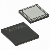
ATMEGA162L-8MC Atmel, ATMEGA162L-8MC Datasheet - Page 77

ATMEGA162L-8MC
Manufacturer Part Number
ATMEGA162L-8MC
Description
IC MCU AVR 16K 3V 8MHZ 44-QFN
Manufacturer
Atmel
Series
AVR® ATmegar
Specifications of ATMEGA162L-8MC
Core Processor
AVR
Core Size
8-Bit
Speed
8MHz
Connectivity
EBI/EMI, SPI, UART/USART
Peripherals
Brown-out Detect/Reset, POR, PWM, WDT
Number Of I /o
35
Program Memory Size
16KB (8K x 16)
Program Memory Type
FLASH
Eeprom Size
512 x 8
Ram Size
1K x 8
Voltage - Supply (vcc/vdd)
2.7 V ~ 5.5 V
Oscillator Type
Internal
Operating Temperature
0°C ~ 70°C
Package / Case
44-VQFN Exposed Pad
Lead Free Status / RoHS Status
Contains lead / RoHS non-compliant
Data Converters
-
- Current page: 77 of 289
- Download datasheet (3Mb)
ATmega162(V/U/L)
• TOSC1/XCK0/OC3A – Port D, Bit 4
TOSC1, Timer Oscillator pin 1: When the AS2 bit in ASSR is set (one) to enable asyn-
chronous clocking of Timer/Counter2, pin PD4 is disconnected from the port, and
becomes the input of the inverting Oscillator Amplifier. In this mode, a crystal Oscillator
is connected to this pin, and the pin can not be used as an I/O pin.
XCK0, USART0 External Clock: The Data Direction Register (DDD4) controls whether
the clock is output (DDD4 set (one)) or input (DDD4 cleared (zero)). The XCK0 pin is
active only when USART0 operates in Synchronous mode.
OC3A, Output Compare Match A output: The PD4 pin can serve as an external output
for the Timer/Counter1 Output Compare A. The pin has to be configured as an output
(DDD4 set (one)) to serve this function. The OC4A pin is also the output pin for the
PWM mode timer function.
• INT1/ICP3 – Port D, Bit 3
INT1, External Interrupt Source 1: The PD3 pin can serve as an external interrupt
source.
ICP3, Input Capture Pin: The PD3 pin can act as an input capture pin for
Timer/Counter3.
• INT0/XCK1 – Port D, Bit 2
INT0, External Interrupt Source 0: The PD2 pin can serve as an external interrupt
source.
XCK1, USART1 External Clock: The Data Direction Register (DDD2) controls whether
the clock is output (DDD2 set (one)) or input (DDD2 cleared (zero)). The XCK1 pin is
active only when USART1 operates in Synchronous mode.
• TXD0 – Port D, Bit 1
TXD0, Transmit Data (Data output pin for USART0). When the USART0 Transmitter is
enabled, this pin is configured as an output regardless of the value of DDD1.
77
2513C–AVR–09/02
Related parts for ATMEGA162L-8MC
Image
Part Number
Description
Manufacturer
Datasheet
Request
R

Part Number:
Description:
Manufacturer:
Atmel Corporation
Datasheet:

Part Number:
Description:
IC AVR MCU 16K 16MHZ 5V 44TQFP
Manufacturer:
Atmel
Datasheet:

Part Number:
Description:
IC AVR MCU 16K 16MHZ 5V 40DIP
Manufacturer:
Atmel
Datasheet:

Part Number:
Description:
IC AVR MCU 16K 16MHZ 5V 44-QFN
Manufacturer:
Atmel
Datasheet:

Part Number:
Description:
IC MCU AVR 16K 5V 16MHZ 44-TQFP
Manufacturer:
Atmel
Datasheet:

Part Number:
Description:
IC MCU AVR 16K 5V 16MHZ 44-QFN
Manufacturer:
Atmel
Datasheet:

Part Number:
Description:
MCU AVR 16KB FLASH 16MHZ 44QFN
Manufacturer:
Atmel
Datasheet:

Part Number:
Description:
MCU AVR 16KB FLASH 16MHZ 44TQFP
Manufacturer:
Atmel
Datasheet:

Part Number:
Description:
IC MCU AVR 16K 5V 16MHZ 44-TQFP
Manufacturer:
Atmel
Datasheet:

Part Number:
Description:
IC MCU AVR 16K 5V 16MHZ 44-QFN
Manufacturer:
Atmel
Datasheet:

Part Number:
Description:
IC MCU AVR 16K 5V 16MHZ 40-DIP
Manufacturer:
Atmel
Datasheet:

Part Number:
Description:
IC MCU AVR 16K 5V 16MHZ 40-DIP
Manufacturer:
Atmel
Datasheet:

Part Number:
Description:
IC MCU AVR 16K 5V 16MHZ 44-TQFP
Manufacturer:
Atmel
Datasheet:


