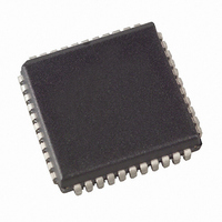
AT89S8253-24JI Atmel, AT89S8253-24JI Datasheet - Page 24

AT89S8253-24JI
Manufacturer Part Number
AT89S8253-24JI
Description
IC 8051 MCU FLASH 12K 44PLCC
Manufacturer
Atmel
Series
89Sr
Datasheet
1.AT89S8253-24PU.pdf
(60 pages)
Specifications of AT89S8253-24JI
Core Processor
8051
Core Size
8-Bit
Speed
24MHz
Connectivity
SPI, UART/USART
Peripherals
POR, WDT
Number Of I /o
32
Program Memory Size
12KB (12K x 8)
Program Memory Type
FLASH
Eeprom Size
2K x 8
Ram Size
256 x 8
Voltage - Supply (vcc/vdd)
2.7 V ~ 5.5 V
Oscillator Type
Internal
Operating Temperature
-40°C ~ 85°C
Package / Case
44-PLCC
Data Bus Width
8 bit
Data Ram Size
256 B
Interface Type
SPI, UART
Maximum Clock Frequency
24 MHz
Number Of Programmable I/os
32
Number Of Timers
3 bit
Operating Supply Voltage
2.7 V to 5.5 V
Maximum Operating Temperature
+ 85 C
Mounting Style
SMD/SMT
Minimum Operating Temperature
- 40 C
Lead Free Status / RoHS Status
Contains lead / RoHS non-compliant
Data Converters
-
Lead Free Status / Rohs Status
No RoHS Version Available
Available stocks
Company
Part Number
Manufacturer
Quantity
Price
Company:
Part Number:
AT89S8253-24JI
Manufacturer:
ATMEL
Quantity:
5 530
Company:
Part Number:
AT89S8253-24JI
Manufacturer:
ATM
Quantity:
3 290
Company:
Part Number:
AT89S8253-24JI
Manufacturer:
ATMEL
Quantity:
13 888
24
AT89S8253
Figure 14-2. SPI Block Diagram
Note:
The SPI has two modes of operation: normal (non-buffered write) and enhanced (buffered
write). In normal mode, writing to the SPI data register (SPDR) of the master CPU starts the SPI
clock generator and the data written shifts out of the MOSI pin and into the MOSI pin of the slave
CPU. Transmission may start after an initial delay while the clock generator waits for the next full
bit slot of the specified baud rate. After shifting one byte, the SPI clock generator stops, setting
the end of transmission flag (SPIF) and transferring the received byte to the read buffer (SPDR).
If both the SPI interrupt enable bit (SPIE) and the serial port interrupt enable bit (ES) are set, an
interrupt is requested. Note that SPDR refers to either the write data buffer or the read data buf-
fer, depending on whether the access is a write or read. In normal mode, because the write
buffer is transparent (and a write access to SPDR will be directed to the shift buffer), any attempt
to write to SPDR while a transmission is in progress will result in a write collision with WCOL set.
However, the transmission will still complete normally, but the new byte will be ignored and a
new write access to SPDR will be necessary.
Enhanced mode is similar to normal mode except that the write buffer holds the next byte to be
transmitted. Writing to SPDR loads the write buffer and sets WCOL to signify that the buffer is
full and any further writes will overwrite the buffer. WCOL is cleared by hardware when the buff-
ered byte is loaded into the shift register and transmission begins. If the master SPI is currently
idle, i.e. if this is the first byte, then after loading SPDR, transmission of the byte starts and
WCOL is cleared immediately. While this byte is transmitting, the next byte may be written to
SPDR. The Load Enable flag (LDEN) in SPSR can be used to determine when transmission has
started. LDEN is asserted during the first four bit slots of a SPI transfer. The master CPU should
first check that LDEN is set and that WCOL is cleared before loading the next byte. In enhanced
mode, if WCOL is set when a transfer completes, i.e. the next byte is available, then the SPI
immediately loads the buffered byte into the shift register, resets WCOL, and continues trans-
mission without stopping and restarting the clock generator. As long as the CPU can keep the
write buffer full in this manner, multiple bytes may be transferred with minimal latency between
bytes.
1. The Write Data Buffer is only used in enhanced SPI mode.
SPI STATUS REGISTER
OSCILLATOR
÷4÷16÷64÷128
SELECT
DIVIDER
SPI CONTROL
SPI INTERRUPT
SPI CLOCK (MASTER)
REQUEST
MSTR
SPE
8
INTERNAL
MSB
DATA BUS
8
8-BIT SHIFT REGISTER
WRITE DATA BUFFER
READ DATA BUFFER
8
SPI CONTROL REGISTER
CLOCK
LOGIC
LSB
CLOCK
(1)
S
M
M
S
S
M
MISO
MOSI
P1.6
P1.5
SCK
P1.4
1.7
SS
3286P–MICRO–3/10


