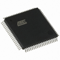
AT89C51SND1C-ROTUL Atmel, AT89C51SND1C-ROTUL Datasheet - Page 90

AT89C51SND1C-ROTUL
Manufacturer Part Number
AT89C51SND1C-ROTUL
Description
IC 8051 MCU FLASH 64K MP3 80TQFP
Manufacturer
Atmel
Series
89Cr
Datasheet
1.AT80C51SND1C-ROTIL.pdf
(213 pages)
Specifications of AT89C51SND1C-ROTUL
Core Processor
8051
Core Size
8-Bit
Speed
40MHz
Connectivity
I²C, IDE/ATAPI, MMC, SPI, UART/USART, USB
Peripherals
Audio, I²S, MP3, PCM, POR, WDT
Number Of I /o
44
Program Memory Size
64KB (64K x 8)
Program Memory Type
FLASH
Ram Size
2.25K x 8
Voltage - Supply (vcc/vdd)
2.7 V ~ 3.3 V
Data Converters
A/D 2x10b
Oscillator Type
External
Operating Temperature
-40°C ~ 85°C
Package / Case
80-TQFP, 80-VQFP
Lead Free Status / RoHS Status
Lead free / RoHS Compliant
Eeprom Size
-
Available stocks
Company
Part Number
Manufacturer
Quantity
Price
- Current page: 90 of 213
- Download datasheet (3Mb)
15.4.4
90
AT8xC51SND1C
Bulk/Interrupt IN Transactions in Ping-pong Mode
All USB retry mechanisms are automatically managed by the USB controller.
Figure 15-12. Bulk/Interrupt IN transactions in Ping-pong mode
An endpoint should be first enabled and configured before being able to send Bulk or Interrupt
packets.
The firmware should fill the FIFO bank 0 with the data to be sent and set the TXRDY bit in the
UEPSTAX register to allow the USB controller to send the data stored in FIFO at the next IN
request concerning the endpoint. The FIFO banks are automatically switched, and the firmware
can immediately write into the endpoint FIFO bank 1.
When the IN packet concerning the bank 0 has been sent and acknowledged by the Host, the
TXCMPL bit is set by the USB controller. This triggers a USB interrupt if enabled. The firmware
should clear the TXCMPL bit before filling the endpoint FIFO bank 0 with new data. The FIFO
banks are then automatically switched.
When the IN packet concerning the bank 1 has been sent and acknowledged by the Host, the
TXCMPL bit is set by the USB controller. This triggers a USB interrupt if enabled. The firmware
should clear the TXCMPL bit before filling the endpoint FIFO bank 1 with new data.
The bank switch is performed by the USB controller each time the TXRDY bit is set by the firm-
ware. Until the TXRDY bit has been set by the firmware for an endpoint bank, the USB controller
will answer a NAK handshake for each IN requests concerning this bank.
Note that in the example above, the firmware clears the Transmit Complete bit (TXCBulk-out-
MPL) before setting the Transmit Ready bit (TXRDY). This is done in order to avoid the firmware
to clear at the same time the TXCMPL bit for for bank 0 and the bank 1.
HOST
IN
IN
IN
IN
ACK
ACK
ACK
DATA0 (n Bytes)
DATA1 (m Bytes)
DATA0 (p Bytes)
NACK
UFI
TXCMPL
TXCMPL
Endpoint FIFO bank 0 - Write Byte 1
Endpoint FIFO bank 0 - Write Byte 2
Endpoint FIFO bank 0 - Write Byte n
Endpoint FIFO bank 1 - Write Byte 1
Endpoint FIFO bank 1 - Write Byte 2
Endpoint FIFO bank 1 - Write Byte m
Endpoint FIFO bank 0 - Write Byte 1
Endpoint FIFO bank 0 - Write Byte 2
Endpoint FIFO bank 0 - Write Byte p
Endpoint FIFO bank 1 - Write Byte 1
C51
Clear TXCMPL
Clear TXCMPL
Set TXRDY
Set TXRDY
Set TXRDY
4109L–8051–02/08
Related parts for AT89C51SND1C-ROTUL
Image
Part Number
Description
Manufacturer
Datasheet
Request
R

Part Number:
Description:
Mp3 Microcontrollers
Manufacturer:
ATMEL Corporation
Datasheet:

Part Number:
Description:
BOARD DEMO MP3 PLAYER
Manufacturer:
Atmel
Datasheet:

Part Number:
Description:
DEV KIT FOR AVR/AVR32
Manufacturer:
Atmel
Datasheet:

Part Number:
Description:
INTERVAL AND WIPE/WASH WIPER CONTROL IC WITH DELAY
Manufacturer:
ATMEL Corporation
Datasheet:

Part Number:
Description:
Low-Voltage Voice-Switched IC for Hands-Free Operation
Manufacturer:
ATMEL Corporation
Datasheet:

Part Number:
Description:
MONOLITHIC INTEGRATED FEATUREPHONE CIRCUIT
Manufacturer:
ATMEL Corporation
Datasheet:

Part Number:
Description:
AM-FM Receiver IC U4255BM-M
Manufacturer:
ATMEL Corporation
Datasheet:

Part Number:
Description:
Monolithic Integrated Feature Phone Circuit
Manufacturer:
ATMEL Corporation
Datasheet:

Part Number:
Description:
Multistandard Video-IF and Quasi Parallel Sound Processing
Manufacturer:
ATMEL Corporation
Datasheet:

Part Number:
Description:
High-performance EE PLD
Manufacturer:
ATMEL Corporation
Datasheet:

Part Number:
Description:
8-bit Flash Microcontroller
Manufacturer:
ATMEL Corporation
Datasheet:

Part Number:
Description:
2-Wire Serial EEPROM
Manufacturer:
ATMEL Corporation
Datasheet:


