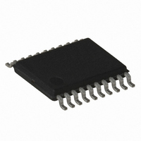
ATTINY167-15XZ Atmel, ATTINY167-15XZ Datasheet - Page 154

ATTINY167-15XZ
Manufacturer Part Number
ATTINY167-15XZ
Description
MCU AVR 16K FLASH 15MHZ 20-TSSOP
Manufacturer
Atmel
Series
AVR® ATtinyr
Datasheet
1.ATTINY167-15MD.pdf
(283 pages)
Specifications of ATTINY167-15XZ
Core Processor
AVR
Core Size
8-Bit
Speed
16MHz
Connectivity
I²C, LIN, SPI, UART/USART, USI
Peripherals
Brown-out Detect/Reset, POR, PWM, Temp Sensor, WDT
Number Of I /o
16
Program Memory Size
16KB (8K x 16)
Program Memory Type
FLASH
Eeprom Size
512 x 8
Ram Size
512 x 8
Voltage - Supply (vcc/vdd)
2.7 V ~ 5.5 V
Data Converters
A/D 11x10b
Oscillator Type
Internal
Operating Temperature
-40°C ~ 125°C
Package / Case
20-TSSOP
For Use With
ATSTK600-SOIC - STK600 SOCKET/ADAPTER FOR SOIC
Lead Free Status / RoHS Status
Lead free / RoHS Compliant
- Current page: 154 of 283
- Download datasheet (5Mb)
154
ATtiny87/ATtiny167
Figure 14-4. Two-wire Mode Operation, Simplified Diagram
Figure 14-4
Slave. It is only the physical layer that is shown since the system operation is highly depen-
dent of the communication scheme used. The main differences between the Master and Slave
operation at this level, is the serial clock generation which is always done by the Master, and
only the Slave uses the clock control unit. Clock generation must be implemented in software,
but the shift operation is done automatically by both devices. Note that only clocking on nega-
tive edge for shifting data is of practical use in this mode. The slave can insert wait states at
start or end of transfer by forcing the SCL clock low. This means that the Master must always
check if the SCL line was actually released after it has generated a positive edge.
Since the clock also increments the counter, a counter overflow can be used to indicate that
the transfer is completed. The clock is generated by the master by toggling the USCK pin via
the PORT Register.
The data direction is not given by the physical layer. A protocol, like the one used by the
TWI-bus, must be implemented to control the data flow.
Figure 14-5. Two-wire Mode, Typical Timing Diagram
SDA
SCL
SLAVE
MASTER
A B
Bit7
Bit7
S
shows two USI units operating in Two-wire mode, one as Master and one as
Bit6
Bit6
C
ADDRESS
Bit5
Bit5
1 - 7
Bit4
Bit4
Bit3
Bit3
R/W
8
Bit2
Bit2
D
Bit1
Bit1
ACK
9
Bit0
Bit0
E
DATA
1 - 8
Two-wire Clock
Control Unit
ACK
9
PORTxn
HOLD
SCL
DATA
1 - 8
SDA
SCL
SDA
SCL
ACK
9
VCC
7728G–AVR–06/10
P
F
Related parts for ATTINY167-15XZ
Image
Part Number
Description
Manufacturer
Datasheet
Request
R

Part Number:
Description:
Manufacturer:
Atmel Corporation
Datasheet:

Part Number:
Description:
Manufacturer:
Atmel Corporation
Datasheet:

Part Number:
Description:
MCU AVR 16K FLASH 15MHZ 32-QFN
Manufacturer:
Atmel
Datasheet:

Part Number:
Description:
IC MCU AVR 16K FLASH 20TSSOP
Manufacturer:
Atmel
Datasheet:

Part Number:
Description:
MCU AVR 16K FLASH 15MHZ 32-QFN
Manufacturer:
Atmel
Datasheet:

Part Number:
Description:
MCU AVR 16K FLASH 15MHZ 20-SOIC
Manufacturer:
Atmel
Datasheet:

Part Number:
Description:
MCU AVR 16K FLASH 15MHZ 20-TSSOP
Manufacturer:
Atmel
Datasheet:

Part Number:
Description:
IC MCU AVR 16K FLASH 20SOIC
Manufacturer:
Atmel
Datasheet:


