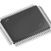
SAF-XC164CS-16F40F BB Infineon Technologies, SAF-XC164CS-16F40F BB Datasheet - Page 20

SAF-XC164CS-16F40F BB
Manufacturer Part Number
SAF-XC164CS-16F40F BB
Description
IC MCU 16BIT FLASH TQFP-100-16
Manufacturer
Infineon Technologies
Series
XC16xr
Datasheet
1.SAF-XC164CS-16F20F_BB.pdf
(80 pages)
Specifications of SAF-XC164CS-16F40F BB
Core Processor
C166SV2
Core Size
16-Bit
Speed
40MHz
Connectivity
CAN, EBI/EMI, SPI, UART/USART
Peripherals
PWM, WDT
Number Of I /o
79
Program Memory Size
128KB (128K x 8)
Program Memory Type
FLASH
Ram Size
8K x 8
Voltage - Supply (vcc/vdd)
2.35 V ~ 2.7 V
Data Converters
A/D 14x8/10b
Oscillator Type
Internal
Operating Temperature
-40°C ~ 85°C
Package / Case
100-LFQFP
Data Bus Width
16 bit
Data Ram Size
8 KB
Interface Type
2xASC, 2xSSC
Maximum Clock Frequency
40 MHz
Number Of Programmable I/os
79
Number Of Timers
11
Operating Supply Voltage
5 V
Maximum Operating Temperature
+ 85 C
Mounting Style
SMD/SMT
Minimum Operating Temperature
- 40 C
On-chip Adc
10 bit, 14 Channel
Packages
PG-TQFP-100
Max Clock Frequency
40.0 MHz
Sram (incl. Cache)
8.0 KByte
Can Nodes
2
A / D Input Lines (incl. Fadc)
14
Program Memory
128.0 KByte
For Use With
B158-H8962-X-X-7600IN - KIT EASY XC164CSMCBX167-NET - BOARD EVAL INFINEON CAN/ETHRNTMCBXC167-BASIC - BOARD EVAL BASIC INFINEON XC16X
Lead Free Status / RoHS Status
Lead free / RoHS Compliant
Eeprom Size
-
Lead Free Status / Rohs Status
Details
Other names
FX164CS16F40FBBNP
FX164CS16F40FBBXT
SAFXC164CS16F40FBBT
SP000094312
SP000224552
FX164CS16F40FBBXT
SAFXC164CS16F40FBBT
SP000094312
SP000224552
XC164CS
Derivatives
Functional Description
3.1
Memory Subsystem and Organization
The memory space of the XC164CS is configured in a Von Neumann architecture, which
means that all internal and external resources, such as code memory, data memory,
registers and I/O ports, are organized within the same linear address space. This
common memory space includes 16 Mbytes and is arranged as 256 segments of
64 Kbytes each, where each segment consists of four data pages of 16 Kbytes each.
The entire memory space can be accessed bytewise or wordwise. Portions of the on-
chip DPRAM and the register spaces (E/SFR) have additionally been made directly
bitaddressable.
The internal data memory areas and the Special Function Register areas (SFR and
ESFR) are mapped into segment 0, the system segment.
The Program Management Unit (PMU) handles all code fetches and, therefore, controls
accesses to the program memories, such as Flash memory, ROM, and PSRAM.
The Data Management Unit (DMU) handles all data transfers and, therefore, controls
accesses to the DSRAM and the on-chip peripherals.
Both units (PMU and DMU) are connected via the high-speed system bus to exchange
data. This is required if operands are read from program memory, code or data is written
to the PSRAM, code is fetched from external memory, or data is read from or written to
external resources, including peripherals on the LXBus (such as TwinCAN). The system
bus allows concurrent two-way communication for maximum transfer performance.
1)
64/128 Kbytes
of on-chip Flash memory or mask-programmable ROM store code
or constant data. The on-chip Flash memory is organized as four 8-Kbyte sectors, one
32-Kbyte sector, and one 64-Kbyte sector. Each sector can be separately write
2)
protected
, erased and programmed (in blocks of 128 Bytes). The complete Flash or
ROM area can be read-protected. A password sequence temporarily unlocks protected
areas. The Flash module combines very fast 64-bit one-cycle read accesses with
protected and efficient writing algorithms for programming and erasing. Thus, program
execution out of the internal Flash results in maximum performance. Dynamic error
correction provides extremely high read data security for all read accesses.
For timing characteristics, please refer to
Section
4.4.2.
2 Kbytes of on-chip Program SRAM (PSRAM) are provided to store user code or data.
The PSRAM is accessed via the PMU and is therefore optimized for code fetches.
1)
2/4 Kbytes
of on-chip Data SRAM (DSRAM) are provided as a storage for general
user data. The DSRAM is accessed via the DMU and is therefore optimized for data
accesses.
2 Kbytes of on-chip Dual-Port RAM (DPRAM) are provided as a storage for user
defined variables, for the system stack, and general purpose register banks. A register
1) Depends on the respective derivative. The derivatives are listed in
Table
1.
2) Each two 8-Kbyte sectors are combined for write-protection purposes.
Data Sheet
18
V2.3, 2006-08


