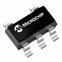
MCP6041T-I/OT Microchip Technology, MCP6041T-I/OT Datasheet - Page 13

MCP6041T-I/OT
Manufacturer Part Number
MCP6041T-I/OT
Description
IC OPAMP 1UA 1.4V SNGLR-R SOT235
Manufacturer
Microchip Technology
Specifications of MCP6041T-I/OT
Slew Rate
0.003 V/µs
Package / Case
SOT-23-5, SC-74A, SOT-25
Amplifier Type
General Purpose
Number Of Circuits
1
Output Type
Rail-to-Rail
Gain Bandwidth Product
14kHz
Current - Input Bias
1pA
Voltage - Input Offset
3000µV
Current - Supply
0.6µA
Current - Output / Channel
20mA
Voltage - Supply, Single/dual (±)
1.4 V ~ 6 V
Operating Temperature
-40°C ~ 85°C
Mounting Type
Surface Mount
Number Of Channels
1
Common Mode Rejection Ratio (min)
60 dB
Input Offset Voltage
3 mV
Input Bias Current (max)
1 pA
Operating Supply Voltage
3 V, 5 V
Maximum Operating Temperature
+ 85 C
Minimum Operating Temperature
- 40 C
Mounting Style
SMD/SMT
Shutdown
No
Supply Voltage (max)
6 V
Supply Voltage (min)
1.4 V
Technology
CMOS
Voltage Gain Db
115 dB
Lead Free Status / RoHS Status
Lead free / RoHS Compliant
-3db Bandwidth
-
Lead Free Status / Rohs Status
Lead free / RoHS Compliant
Other names
MCP6041T-I/OT
MCP6041T-I/OTTR
MCP6041T-I/OTTR
Available stocks
Company
Part Number
Manufacturer
Quantity
Price
Company:
Part Number:
MCP6041T-I/OT
Manufacturer:
KEMET
Quantity:
500 000
Company:
Part Number:
MCP6041T-I/OT
Manufacturer:
Microchip Technology
Quantity:
138 832
Part Number:
MCP6041T-I/OT
Manufacturer:
MICROCH1P
Quantity:
20 000
4.2
There are two specifications that describe the output
swing capability of the MCP6041/2/3/4 family of op
amps. The first specification (Maximum Output Voltage
Swing) defines the absolute maximum swing that can
be achieved under the specified load condition. Thus,
the output voltage swings to within 10 mV of either sup-
ply rail with a 50 kΩ load to V
how the output voltage is limited when the input goes
beyond the linear region of operation.
The second specification that describes the output
swing capability of these amplifiers is the Linear Output
Voltage Range. This specification defines the maxi-
mum output swing that can be achieved while the
amplifier still operates in its linear region. To verify
linear operation in this range, the large signal DC
Open-Loop Gain (A
supply rails. The measurement must meet the specified
A
4.3
The MCP6041/2/3/4 op amp family has outstanding
quiescent current, which supports battery-powered
applications. There is minimal quiescent current
glitching when Chip Select (CS) is raised or lowered.
This prevents excessive current draw, and reduced
battery life, when the part is turned off or on.
Heavy resistive loads at the output can cause
excessive battery drain. Driving a DC voltage of 2.5V
across a 100 kΩ load resistor will cause the supply cur-
rent to increase by 25 µA, depleting the battery 43
times as fast as I
High frequency signals (fast edge rate) across
capacitive loads will also significantly increase supply
current. For instance, a 0.1 µF capacitor at the output
presents an AC impedance of 15.9 kΩ (1/2πfC) to a
100 Hz sinewave. It can be shown that the average
power drawn from the battery by a 5.0 V
(1.77 V
EQUATION 4-1:
This will drain the battery 18 times as fast as I
© 2008 Microchip Technology Inc.
OL
P
condition in the specification table.
Supply
rms
Rail-to-Rail Output
Output Loads and Battery Life
), under these conditions, is
= (5V)(0.6 µA + 5.0V
= 3.0 µW + 50 µW
= (V
DD
Q
- V
(0.6 µA, typical) alone.
OL
SS
) is measured at points inside the
) (I
Q
+ V
DD
p-p
L(p-p)
/2.
·
100Hz
Figure 2-10
f C
L
)
·
p-p
0.1µF)
sinewave
Q
alone.
shows
4.4
Driving large capacitive loads can cause stability
problems for voltage feedback op amps. As the load
capacitance increases, the feedback loop’s phase
margin decreases and the closed-loop bandwidth is
reduced. This produces gain peaking in the frequency
response, with overshoot and ringing in the step
response. A unity gain buffer (G = +1) is the most
sensitive to capacitive loads, although all gains show
the same general behavior.
When driving large capacitive loads with these op
amps (e.g., > 60 pF when G = +1), a small series
resistor at the output (R
feedback loop’s phase margin (stability) by making the
output load resistive at higher frequencies. The
bandwidth will be generally lower than the bandwidth
with no capacitive load.
FIGURE 4-3:
stabilizes large capacitive loads.
Figure 4-4
different capacitive loads and gains. The x-axis is the
normalized load capacitance (C
circuit’s noise gain. For non-inverting gains, G
Signal Gain are equal. For inverting gains, G
1+|Signal Gain| (e.g., -1 V/V gives G
FIGURE 4-4:
for Capacitive Loads.
After selecting R
resulting frequency response peaking and step
response overshoot. Modify R
response is reasonable. Bench evaluation and
simulations with the MCP6041/2/3/4 SPICE macro
model are helpful.
100,000
10,000
V
1,000
100k
IN
10k
1k
1.E+01
Capacitive Loads
10p
gives recommended R
Normalized Load Capacitance; C
MCP604X
MCP6041/2/3/4
ISO
for your circuit, double check the
1.E+02
100p
Output Resistor, R
Recommended R
ISO
in
G
G
G
Figure
N
N
N
R
= +1
= +2
L
C
+5
ISO
ISO
/G
L
1.E+03
N
1n
’s value until the
), where G
N
DS21669C-page 13
4-3) improves the
ISO
= +2 V/V).
L
/G
ISO
values for
N
ISO
V
(F)
N
OUT
1.E+04
Values
and the
N
10n
is the
N
is


