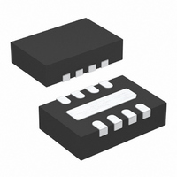
LTC6102CDD-1#PBF Linear Technology, LTC6102CDD-1#PBF Datasheet - Page 18

LTC6102CDD-1#PBF
Manufacturer Part Number
LTC6102CDD-1#PBF
Description
IC AMP CURRENT SENSE 8-DFN
Manufacturer
Linear Technology
Datasheet
1.LTC6102CDDPBF.pdf
(26 pages)
Specifications of LTC6102CDD-1#PBF
Amplifier Type
Current Sense
Number Of Circuits
1
Gain Bandwidth Product
200kHz
Current - Input Bias
60pA
Voltage - Input Offset
3µV
Current - Supply
420µA
Current - Output / Channel
1mA
Voltage - Supply, Single/dual (±)
4 V ~ 60 V
Operating Temperature
0°C ~ 70°C
Mounting Type
Surface Mount
Package / Case
8-DFN
No. Of Amplifiers
1
Input Bias Current
3nA
Output Current Per Channel
1mA
Input Offset Voltage
10µV
Bandwidth
200kHz
Supply Voltage Range
4V To 60V
Supply Current
650µA
Rohs Compliant
Yes
Lead Free Status / RoHS Status
Lead free / RoHS Compliant
Output Type
-
-3db Bandwidth
-
Slew Rate
-
Available stocks
Company
Part Number
Manufacturer
Quantity
Price
APPLICATIONS INFORMATION
LTC6102
LTC6102-1/LTC6102HV
the allowed output current. The gain is still controlled by
R
the input signal as it is translated to the output. Finally,
the input may be a voltage source rather than a sense
resistor, as shown in Figure 8. This circuit allows the
translation of a wide variety of input signals across the
entire supply range of the LTC6102 with only a tiny offset
error while retaining simple gain control set by R
Again, very large voltages may be sensed as long as R
is chosen so that I
current. For example, V
1k, or as large as 10V with R
input and a 5V maximum output, R
will allow the LTC6102HV to translate V
common mode voltage of up to 100V. For the case where
a large input resistor is used, a similar resistor in series
with +IN will reduce error due to input bias current.
Reverse Supply Current
Some applications may be tested with reverse-polarity
supplies due to an expectation of this type of fault during
operation. The LTC6102 is not protected internally from
external reversal of supply polarity. To prevent damage
that may occur during this condition, a Schottky diode
should be added in series with V
limit the reverse current through the LTC6102. Note that
this diode will limit the low voltage performance of the
18
OUT
V
/R
V
CM
IN
IN
V
, so either gain or attenuation may be applied to
+
V
Figure 8. Voltage Level-Shift Circuit
R
OUT
IN
= V
+IN
OUT
V
IN
–
•
R
LTC6102
R
does not exceed the allowed output
OUT
IN
IN
+
may be as large as 1V with R
IN
= 10k. For a 10V maximum
–
IN
–
(Figure 9). This will
= 10k and R
V
OUT
–INS
–INF
V
REG
IN
+
to V
R
OUT
OUT
0.1μF
V
OUT
OUT
OUT
6102 F08
with a
/R
= 5k
IN
IN
IN
=
.
LTC6102 by effectively reducing the supply voltage to the
part by V
In addition, if the output of the LTC6102 is wired to a device
that will effectively short it to high voltage (such as through
an ESD protection clamp) during a reverse supply condi-
tion, the LTC6102’s output should be connected through
a resistor or Schottky diode (Figure 10).
Response Time
The LTC6102 is designed to exhibit fast response to inputs
for the purpose of circuit protection or signal transmission.
This response time will be affected by the external circuit
in two ways, delay and speed.
V
BATT
O
D
L
A
Figure 9. Schottky Prevents Damage During Supply Reversal
R
SENSE
+IN
V
D
D1
–
.
V
Figure 10. Additional Resistor R3 Protects
Output During Supply Reversal
BATT
LTC6102
L
O
A
D
R
SENSE
+
+IN
–
V
D1
–
LTC6102
+
–INS
–INF
V
V
OUT
+
REG
–
0.1μF
R2
4.99k
R1
100Ω
R3
1k
–INS
–INF
V
V
OUT
+
REG
0.1μF
R1
100Ω
6102 F10
R2
4.99k
6102 F09
ADC
6102fd


