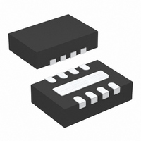
LTC6102CDD-1#PBF Linear Technology, LTC6102CDD-1#PBF Datasheet - Page 5

LTC6102CDD-1#PBF
Manufacturer Part Number
LTC6102CDD-1#PBF
Description
IC AMP CURRENT SENSE 8-DFN
Manufacturer
Linear Technology
Datasheet
1.LTC6102CDDPBF.pdf
(26 pages)
Specifications of LTC6102CDD-1#PBF
Amplifier Type
Current Sense
Number Of Circuits
1
Gain Bandwidth Product
200kHz
Current - Input Bias
60pA
Voltage - Input Offset
3µV
Current - Supply
420µA
Current - Output / Channel
1mA
Voltage - Supply, Single/dual (±)
4 V ~ 60 V
Operating Temperature
0°C ~ 70°C
Mounting Type
Surface Mount
Package / Case
8-DFN
No. Of Amplifiers
1
Input Bias Current
3nA
Output Current Per Channel
1mA
Input Offset Voltage
10µV
Bandwidth
200kHz
Supply Voltage Range
4V To 60V
Supply Current
650µA
Rohs Compliant
Yes
Lead Free Status / RoHS Status
Lead free / RoHS Compliant
Output Type
-
-3db Bandwidth
-
Slew Rate
-
Available stocks
Company
Part Number
Manufacturer
Quantity
Price
SYMBOL
V
I
t
t
f
ELECTRICAL CHARACTERISTICS
SYMBOL
V
V
ΔV
I
PSRR
V
V
I
t
BW
e
the full operating temperature range, otherwise specifi cations are at T
details), V
operating temperature range, otherwise specifi cations are at T
V
ELECTRICAL CHARACTERISTICS
BEN
ON
OFF
S
B
OUT
r
N
ENH
+
OS
SENSE(MAX)
OUT
+
OS
= 12V, V
/ΔT
+
–
= 12V, V
PARAMETER
Enable Input Voltage High
(LTC6102-1 Only)
Enable Input Pin Current
(LTC6102-1 Only)
Turn-On Time (LTC6102-1 Only)
Turn-Off Time (LTC6102-1 Only) V
Sampling Frequency
PARAMETER
Supply Voltage Range
Input Offset Voltage
(Note 3)
Input Offset Voltage
(Note 4)
Input Offset Voltage Drift (Note 3) V
Input Bias Current (Note 5)
Power Supply Rejection Ratio
Input Sense Voltage Full Scale
(V
Maximum Output Voltage
Maximum Output Current
Input Step Response (to 2.5V on a
5V Output Step)
Signal Bandwidth
Input Noise Voltage
= 0V unless otherwise noted.
+
– V
+IN
–
)
= 0V, V
EN
= 2.2V unless otherwise noted.
CONDITIONS
V
V
Final Value
Than 10% of Nominal Value
EN
EN
EN
CONDITIONS
V
V
R
LTC6102HVC, LTC6102HVI
LTC6102HVH
V
V
Error <1%, R
V
6V ≤ V
V
ΔV
R
V
I
I
0.1Hz to 10Hz
OUT
OUT
SENSE
SENSE
SENSE
IN
SENSE
SENSE
SENSE
+
IN
+
6V ≤ V
V
6V ≤ V
V
LTC6102HVC, LTC6102HVI
LTC6102HVH
6V ≤ V
V
12V ≤ V
V
= 0V to 9V
= 2.2V, V
= 0.8V, V
SENSE
= 5V, R
= 5V
+
+
+
+
= 40k, V
= 100Ω, R
= 200μA, R
= 1mA, R
= 5V
= 5V
= 5V
= 5V
+
= 100μV
= 100μV
= 100μV
= 100μV, V
= 100μV, V
= 2mV, R
≤ 100V, R
+
+
+
= 100mV Transient, 6V ≤ V
+
IN
≤ 100V
≤ 100V
≤ 100V
SENSE
SENSE
≤ 100V
SENSE
= 10Ω, R
IN
IN
OUT
= 10k, R
IN
OUT
= 100Ω, R
(LTC6102, LTC6102-1) The
(LTC6102HV) The
= 1mV, Output Settles to Within 1% of
= 1mV, Supply Current Drops to Less
IN
+
+
= 2mV
= 4.99k, I
= 100Ω, R
= 6V to 100V
= 5V to 100V
= 1k, R
= 100k
A
OUT
= 25°C. R
OUT
= 1k, V
OUT
OUT
= 10k
OUT
OUT
A
= 4.99k
= 1k, V
= 25°C. R
= 100μA
SENSE
= 4.99k
IN
+
= 10Ω, R
≤ 100V,
l
SENSE
= 11mV
denotes the specifi cations which apply over the full
LTC6102-1/LTC6102HV
IN
= 1.1V
= 10Ω, R
OUT
l
denotes the specifi cations which apply over
= 10k, V
OUT
l
l
l
l
l
l
l
l
l
l
l
l
l
l
= 10k, V
SENSE
MIN
MIN
130
125
120
115
2.2
0.5
+
5
2
1
8
3
1
= V
SENSE
+
(see Figure 1 for details),
+
TYP
500
100
TYP
150
140
140
200
1.5
10
25
25
60
= V
3
5
3
5
1
2
LTC6102
+
(see Figure 1 for
MAX
MAX
100
10
25
35
50
50
75
20
8
3
UNITS
UNITS
nV/°C
nV/°C
μV
6102fd
5
kHz
kHz
kHz
mA
mA
P-P
μA
μV
μV
μV
μV
pA
nA
nA
dB
dB
dB
dB
μs
μs
μs
μs
V
V
V
V
V
V


