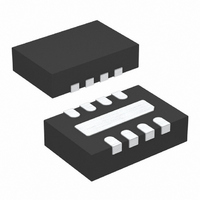
LTC6102IDD-1#PBF Linear Technology, LTC6102IDD-1#PBF Datasheet - Page 10

LTC6102IDD-1#PBF
Manufacturer Part Number
LTC6102IDD-1#PBF
Description
IC AMP CURRENT SENSE 8-DFN
Manufacturer
Linear Technology
Datasheet
1.LTC6102CDDPBF.pdf
(26 pages)
Specifications of LTC6102IDD-1#PBF
Amplifier Type
Current Sense
Number Of Circuits
1
Gain Bandwidth Product
200kHz
Current - Input Bias
60pA
Voltage - Input Offset
3µV
Current - Supply
420µA
Current - Output / Channel
1mA
Voltage - Supply, Single/dual (±)
4 V ~ 60 V
Operating Temperature
-40°C ~ 85°C
Mounting Type
Surface Mount
Package / Case
8-DFN
No. Of Amplifiers
1
Input Bias Current
3nA
Output Current Per Channel
1mA
Input Offset Voltage
10µV
Bandwidth
200kHz
Supply Voltage Range
4V To 60V
Supply Current
650µA
Rohs Compliant
Yes
Lead Free Status / RoHS Status
Lead free / RoHS Compliant
Output Type
-
-3db Bandwidth
-
Slew Rate
-
LTC6102
LTC6102-1/LTC6102HV
PIN FUNCTIONS
–INS (Pin 1): Amplifi er Inverting Input. When tied to –INF ,
the internal sense amplifi er will drive –INS to the same
potential as +IN.
–INF (Pin 2): Force Input. This pin carries the input
current from R
resistor (R
I
ternal R
V
EN (Pin 3, LTC6102-1 Only): Enable Pin, Referenced to
the Negative Supply. When the enable pin is pulled high,
the LTC6102-1 is active. When the enable pin is pulled low
or left fl oating, the LTC6102-1 is disabled.
OUT (Pin 4): Open-Drain Current output. OUT will source
a current that is proportional to the sense voltage into
an external resistor. I
–INF .
10
OUT
–
(Pin 3, LTC6102/LTC6102HV Only): Negative Supply.
= V
SENSE
SENSE
IN
) tied from V
.
/R
IN
IN
and must be tied to –INS near R
. V
SENSE
OUT
+
is the same current that enters
to –INF sets the output current
is the voltage across the ex-
IN
. A
V
V
larger) capacitor should be tied from V
not designed to drive external circuits.
V
through this pin.
+IN (Pin 8): Amplifi er Noninverting Input. Must be tied
to the system load end of the sense resistor. The +IN pin
has an internal 5k series resistor designed to allow large
input voltage transients or accidental disconnection of the
sense resistor. This pin can be held up to 20V below the
–INS pin indefi nitely, or up to 60V below the –INS pin for
up to one second (see Absolute Maximum Ratings).
Exposed Pad (Pin 9, DFN Only): V
must be soldered to PCB.
–
REG
+
(Pin 5): Negative Supply.
(Pin 7): Positive Supply. Supply current is drawn
(Pin 6): Internal Regulated Supply. A 0.1μF (or
–
. The Exposed Pad
REG
to V
+
. V
REG
6102fd
is


