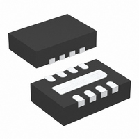
LTC6102IDD-1#PBF Linear Technology, LTC6102IDD-1#PBF Datasheet - Page 12

LTC6102IDD-1#PBF
Manufacturer Part Number
LTC6102IDD-1#PBF
Description
IC AMP CURRENT SENSE 8-DFN
Manufacturer
Linear Technology
Datasheet
1.LTC6102CDDPBF.pdf
(26 pages)
Specifications of LTC6102IDD-1#PBF
Amplifier Type
Current Sense
Number Of Circuits
1
Gain Bandwidth Product
200kHz
Current - Input Bias
60pA
Voltage - Input Offset
3µV
Current - Supply
420µA
Current - Output / Channel
1mA
Voltage - Supply, Single/dual (±)
4 V ~ 60 V
Operating Temperature
-40°C ~ 85°C
Mounting Type
Surface Mount
Package / Case
8-DFN
No. Of Amplifiers
1
Input Bias Current
3nA
Output Current Per Channel
1mA
Input Offset Voltage
10µV
Bandwidth
200kHz
Supply Voltage Range
4V To 60V
Supply Current
650µA
Rohs Compliant
Yes
Lead Free Status / RoHS Status
Lead free / RoHS Compliant
Output Type
-
-3db Bandwidth
-
Slew Rate
-
APPLICATIONS INFORMATION
LTC6102
LTC6102-1/LTC6102HV
The LTC6102 high side current sense amplifi er (Figure 1)
provides accurate monitoring of current through a user-
selected sense resistor. The sense voltage is amplifi ed by
a user-selected gain and level shifted from the positive
power supply to a ground-referred output. The output
signal is analog and may be used as is or processed with
an output fi lter.
Theory of Operation
An internal sense amplifi er loop forces –INS to have the
same potential as +IN. Connecting an external resistor,
R
that is the same as the sense voltage across R
corresponding current, V
The high impedance inputs of the sense amplifi er will not
conduct this input current, so it will fl ow through the –INF
pin and an internal MOSFET to the output pin.
The output current can be transformed into a voltage by
adding a resistor from OUT to V
then V
Useful Gain Confi gurations
Selection of External Current Sense Resistor
The external sense resistor, R
on the function of a current sensing system and must be
chosen with care.
First, the power dissipation in the resistor should be
considered. The system load current will cause both heat
dissipation and voltage loss in R
resistor should be as small as possible while still providing
the input dynamic range required by the measurement.
Note that input dynamic range is the difference between
the maximum input signal and the minimum accurately
reproduced signal, and is limited primarily by input DC
offset of the internal amplifi er of the LTC6102. In addition,
R
12
IN
SENSE
, between –INS and V
GAIN
1000
4990
200
500
O
must be small enough that V
= V
–
+ I
49.9Ω
20Ω
10Ω
R
1Ω
OUT
IN
• R
OUT
4.99k
SENSE
R
10k
10k
10k
+
OUT
.
forces a potential across R
SENSE
/R
SENSE
IN
–
. The output voltage is
, has a signifi cant effect
, will fl ow through R
SENSE
. As a result, the sense
V
SENSE
does not exceed
25mV
10mV
AT V
5mV
1mV
OUT
SENSE
= 5V
. A
IN
IN
.
the maximum sense voltage specifi ed by the LTC6102 or
the sense resistor, even under peak load conditions. As
an example, an application may require that the maximum
sense voltage be 100mV. If this application is expected
to draw 20A at peak load, R
than 5mΩ.
Once the maximum R
minimum sense resistor value will be set by the resolu-
tion or dynamic range required. The minimum signal
that can be accurately represented by this sense amp is
limited by the input offset. As an example, the LTC6102
has a typical input offset of 3μV. If the minimum current
is 1mA, a sense resistor of 3mΩ will set V
This is the same value as the input offset. A larger sense
resistor will reduce the error due to offset by increasing
the sense voltage for a given load current.
For this example, choosing a 5mΩ R
the dynamic range and provide a system that has 100mV
across the sense resistor at peak load (20A), while input
offset causes an error equivalent to only 0.6mA of load
current.
Peak dissipation is 2W. If a 0.5mΩ sense resistor is em-
ployed, then the effective current error is 6mA (0.03%
of full-scale), while the peak sense voltage is reduced to
10mV at 20A, dissipating only 200mW.
The low offset and corresponding large dynamic range of
the LTC6102 make it more fl exible than other solutions
in this respect. The 3μV typical offset gives 100dB of dy-
namic range for a sense voltage that is limited to 300mV
max, and over 116dB of dynamic range if a maximum of
2V is allowed.
The previous example assumes that a large output dynamic
range is required. For circuits that do not require large
dynamic range, the wide input range of the LTC6102 may
be used to reduce the size of the sense resistor, reducing
power loss and increasing reliability. For example, in a
100A circuit requiring 60dB of dynamic range, the input
offset and drift of most current-sense solutions will require
that the shunt be chosen so that the sense voltage is at
least 100mV at full scale so that the minimum input is
greater than 100μV. This will cause power dissipation in
excess of 10W at full scale! That much power loss can put
SENSE
SENSE
value is determined, the
should be no more
SENSE
will maximize
SENSE
to 3μV.
6102fd


