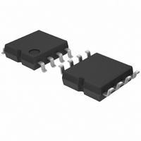
BD7542F-E2 Rohm Semiconductor, BD7542F-E2 Datasheet - Page 18

BD7542F-E2
Manufacturer Part Number
BD7542F-E2
Description
OP AMP I/O FULL SWING HV 8-SOP
Manufacturer
Rohm Semiconductor
Specifications of BD7542F-E2
Slew Rate
0.6 V/µs
Amplifier Type
General Purpose
Number Of Circuits
2
Output Type
Rail-to-Rail
Gain Bandwidth Product
600kHz
Current - Input Bias
1pA
Voltage - Input Offset
1000µV
Current - Supply
400µA
Current - Output / Channel
1mA
Voltage - Supply, Single/dual (±)
5 V ~ 14.5 V
Operating Temperature
-40°C ~ 85°C
Mounting Type
Surface Mount
Package / Case
8-SOP
Op Amp Type
CMOS
No. Of Amplifiers
2
Bandwidth
0.6MHz
Supply Voltage Range
± 2.5V To ± 7.25V
Amplifier Case Style
SOIC
No. Of Pins
8
Operating Temperature Range
-40°C To +85°C
Number Of Channels
2
Common Mode Rejection Ratio (min)
45 dB
Input Offset Voltage
9 mV
Input Bias Current (max)
1 pA
Operating Supply Voltage
9 V, 12 V
Supply Current
0.65 mA
Maximum Operating Temperature
+ 85 C
Minimum Operating Temperature
- 40 C
Dual Supply Voltage
+/- 3 V, +/- 5 V
Maximum Dual Supply Voltage
+/- 7.25 V
Minimum Dual Supply Voltage
+/- 2.5 V
Mounting Style
SMD/SMT
Shutdown
No
Supply Voltage (max)
14.5 V
Supply Voltage (min)
5 V
Technology
CMOS
Voltage Gain Db
95 dB
Lead Free Status / RoHS Status
Lead free / RoHS Compliant
-3db Bandwidth
-
Lead Free Status / Rohs Status
Lead free / RoHS Compliant
Other names
BD7542F-E2TR
Available stocks
Company
Part Number
Manufacturer
Quantity
Price
Company:
Part Number:
BD7542F-E2
Manufacturer:
Rohm
Quantity:
4 900
Part Number:
BD7542F-E2
Manufacturer:
ROHM/罗姆
Quantity:
20 000
BD7561G,BD7561SG,BD7541G,BD7541SG,
BD7562F/FVM,BD7562SF/FVM, BD7542F/FVM,BD7542SF/FVM
●N0tes for use
© 2009 ROHM Co., Ltd. All rights reserved.
www.rohm.com
1) Absolute maximum ratings
2) Applied voltage to the input terminal
3) Operating power supply (split power supply/single power supply)
4) Power dissipation (Pd)
5) Short circuits between pins and incorrect mounting
6) Using under strong electromagnetic field
7) Usage of IC
8) Testing IC on the set board
9) The IC destruction caused by capacitive load
10) Decupling capacitor
11) Latch up
Absolute maximum ratings are the values which indicate the limits,within which the given voltage range can be safely
charged to the terminal.However, it does not guarantee the circuit operation.
For normal circuit operation of voltage comparator, please input voltage for its input terminal within input common mode
voltage VDD+0.3[V].Then, regardless of power supply voltage,VSS-0.3[V] can be applied to inputterminals without
deterioration or destruction of its characteristics.
The voltage comparator operates if a given level of voltage is applied between VDD and VSS. Therefore, the operational
amplifier can be operated under single power supply or split power supply.
If the IC is used under excessive power dissipation. An increase in the chip temperature will cause deterioration of the
radical characteristics of IC. For example, reduction of current capability. Take consideration of the effective power
dissipation andthermal design with a sufficient margin. Pd is reference to the provided power dissipation curve.
Short circuits between pins and incorrect mounting when mounting the IC on a printed circuits board, take notice of the
direction and positioning of the IC.If IC is mounted erroneously, It may be damaged. Also, when a foreign object is inserted
between output, between output and VDD terminal or VSS terminal which causes short circuit, the IC may be damaged.
Be careful when using the IC under strong electromagnetic field because it may malfunction.
When stress is applied to the IC through warp of the printed circuit board, The characteristics may fluctuate due to the
piezo effect. Be careful of the warp of the printed circuit board.
When testing IC on the set board, in cases where the capacitor is connected to the low impedance,make sure to discharge
per fabrication because there is a possibility that IC may be damaged by stress.
When removing IC from the set board, it is essential to cut supply voltage.As a countermeasure against the static
electricity, observe proper grounding during fabrication processand take due care when carrying and storage it.
The transistors in circuits may be damaged when VDD terminal and VSS terminal is shorted with the charged output
terminal capacitor. When IC is used as a operational amplifier or as an application circuit,where oscillation is not activated
by an output capacitor, the output capacitor must be kept below 0.1[μF] in order to prevent the damage mentioned above.
Insert the deculing capacitance between VDD and VSS, for stable operation of operational amplifier.
Be careful of input vltage that exceed the VDD and VSS. When CMOS device have sometimes occur latch up operation.
And protect the IC from abnormaly noise.
18/20
Technical Note
2009.05 - Rev.A


