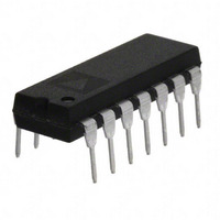
OP470GPZ Analog Devices Inc, OP470GPZ Datasheet - Page 14

OP470GPZ
Manufacturer Part Number
OP470GPZ
Description
IC OPAMP GP 6MHZ QUAD LN 14DIP
Manufacturer
Analog Devices Inc
Specifications of OP470GPZ
Slew Rate
2 V/µs
Amplifier Type
General Purpose
Number Of Circuits
4
Gain Bandwidth Product
6MHz
Current - Input Bias
25nA
Voltage - Input Offset
400µV
Current - Supply
9mA
Voltage - Supply, Single/dual (±)
9 V ~ 36 V, ±4.5 V ~ 18 V
Operating Temperature
-40°C ~ 85°C
Mounting Type
Through Hole
Package / Case
14-DIP (0.300", 7.62mm)
Op Amp Type
General Purpose
No. Of Amplifiers
4
Bandwidth
6MHz
Supply Voltage Range
± 4.5V To ± 18V
Amplifier Case Style
DIP
No. Of Pins
14
Channel Separation
125
Common Mode Rejection Ratio
100
Current, Input Bias
25 nA
Current, Input Offset
12 nA
Current, Supply
9 mA
Impedance, Thermal
33 °C/W
Number Of Amplifiers
Quad
Package Type
PDIP-14
Resistance, Input
0.4 Megohms (Differential), 11 Gigaohms (Common-Mode)
Temperature, Operating, Range
-40 to +85 °C
Voltage, Gain
1700 V/mV
Voltage, Input
±11, ±12 V
Voltage, Noise
3.8 nV/sqrt Hz
Voltage, Offset
0.4 mV
Voltage, Output, High
+13 V
Voltage, Output, Low
-13 V
Voltage, Supply
±15 V
Lead Free Status / RoHS Status
Lead free / RoHS Compliant
Output Type
-
Current - Output / Channel
-
-3db Bandwidth
-
Lead Free Status / Rohs Status
RoHS Compliant part
Electrostatic Device
Available stocks
Company
Part Number
Manufacturer
Quantity
Price
Company:
Part Number:
OP470GPZ
Manufacturer:
AD
Quantity:
1 200
Part Number:
OP470GPZ
Manufacturer:
ADI/亚德诺
Quantity:
20 000
OP470
SQUELCH AMPLIFIER
The circuit of Figure 17 is a simple squelch amplifier that uses a
FET switch to cut off the output when the input signal falls
below a preset limit.
The input signal is sampled by a peak detector with a time
constant set by C1 and R6. When the output of the peak detector
(Vp), falls below the threshold voltage, (VTH), set by R8, the
comparator formed by op amp C switches from V– to V+. This
drives the gate of the N-channel FET high, turning it ON, re-
ducing the gain of the inverting amplifier formed by op amp A
to zero.
V
IN
2k
2k
R1
R3
100k
Figure 17. Squelch Amplifier
R5
= 1 SECOND
1/4
OP470E
A
1/4
OP470E
B
10k
10k
R2
R4
2N5434
1N4148
D1
V
OUT
– –5V
C1
1 F
V+
1N4148
IN
D2
R6
1M
10k
R6
R7
10k
1/4
OP470E
C
10M
10 F
+
R4
C2
–14–
FIVE-BAND LOW-NOISE STEREO GRAPHIC EQUALIZER
The graphic equalizer circuit shown in Figure 18 provides 15 dB
of boost or cut over a 5-band range. Signal-to-noise ratio over a
20 kHz bandwidth is better than 100 dB referred to a 3 V rms
input. Larger inductors can be replaced by active inductors but
this reduces the signal-to-noise ratio.
V
IN
Figure 18. Five-Band Low Noise Graphic Equalizer
0.47 F
47k
C1
R1
680
680
680
680
680
R11
R3
R5
R7
R9
TANTALUM
TANTALUM
TANTALUM
TANTALUM
TANTALUM
1/4
OP470E
0.022 F
0.047 F
0.22 F
6.8 F
+
+
+
+
+
1 F
C2
C3
C4
C5
C6
1H
1H
1H
1H
1H
L1
L2
L3
L4
L5
3.3k
R2
1k
1k
1k
1k
1k
R4
R4
R4
R4
R4
200Hz
800Hz
60Hz
3kHz
10kHz
1/4
OP470E
3.3k
R13
100
R14
REV. B
V
OUT


