AD524ADZ Analog Devices Inc, AD524ADZ Datasheet - Page 2
AD524ADZ
Manufacturer Part Number
AD524ADZ
Description
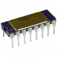
IC AMP INST 1MHZ PREC LN 16CDIP
Manufacturer
Analog Devices Inc
Type
Precisionr
Specifications of AD524ADZ
Amplifier Type
Instrumentation
Number Of Circuits
1
Slew Rate
5 V/µs
Gain Bandwidth Product
1MHz
-3db Bandwidth
1MHz
Current - Input Bias
50nA
Voltage - Input Offset
250µV
Current - Supply
3.5mA
Voltage - Supply, Single/dual (±)
±6 V ~ 18 V
Operating Temperature
-25°C ~ 85°C
Mounting Type
Through Hole
Package / Case
16-CDIP (0.300", 7.62mm)
Bandwidth
25 MHz
Common Mode Rejection Ratio
110
Current, Input Bias
±50 nA
Current, Input Offset
±35 nA
Current, Supply
3.5 mA (Quiescent)
Package Type
SBDIP-16
Power Dissipation
450 mW
Resistance, Input
20 Kilohms
Temperature, Operating, Range
-25 to +85 °C
Voltage, Gain
1-1000 V/V
Voltage, Input
<36 V
Voltage, Input Offset
250 μV
Voltage, Noise
7 nV/sqrt Hz (Input), 90 nV/sqrt Hz (Output)
Voltage, Supply
±15 V
No. Of Amplifiers
5
Input Offset Voltage
250µV
Gain Db Min
1dB
Amplifier Output
Single Ended
Cmrr
110dB
Supply Voltage Range
± 6V To ± 18V
Rohs Compliant
Yes
Lead Free Status / RoHS Status
Lead free / RoHS Compliant
Output Type
-
Current - Output / Channel
-
Lead Free Status / Rohs Status
RoHS Compliant part
Electrostatic Device
Available stocks
Company
Part Number
Manufacturer
Quantity
Price
Company:

Part Number:
AD524ADZ
Manufacturer:
AD
Quantity:
1 000
Company:
Part Number:
AD524ADZ
Manufacturer:
AD
Quantity:
1 000
Part Number:
AD524ADZ
Manufacturer:
ADI/亚德诺
Quantity:
20 000


TABLE OF CONTENTS
Features .............................................................................................. 1
Functional Block Diagram .............................................................. 1
General Description ......................................................................... 1
Product Highlights ........................................................................... 1
Revision History ............................................................................... 2
Specifications ..................................................................................... 3
Absolute Maximum Ratings ............................................................ 8
Typical Performance Characteristics ............................................. 9
Theory of Operation ...................................................................... 15
REVISION HISTORY
11/07—Rev. E to Rev. F
Updated Format .................................................................. Universal
Changes to General Description .................................................... 1
Changes to Figure 1 .......................................................................... 1
Changes to Figure 3 and Figure 4 Captions .................................. 8
Changes to Error Budget Analysis Section ................................. 21
Changes to Ordering Guide .......................................................... 25
4/99—Rev. D to Rev. E
AD524
Connection Diagrams .................................................................. 8
ESD Caution .................................................................................. 8
Test Circuits ................................................................................. 14
Input Protection .......................................................................... 15
Rev. F | Page 2 of 28
Outline Dimensions ....................................................................... 24
Input Offset and Output Offset ................................................ 15
Gain .............................................................................................. 16
Input Bias Currents .................................................................... 17
Common-Mode Rejection ........................................................ 17
Grounding ................................................................................... 18
Sense Terminal ............................................................................ 18
Reference Terminal .................................................................... 18
Programmable Gain ................................................................... 20
Autozero Circuits ....................................................................... 20
Error Budget Analysis ................................................................ 21
Ordering Guide .......................................................................... 25
Related parts for AD524ADZ
Image
Part Number
Description
Manufacturer
Datasheet
Request
R

Part Number:
Description:
±1.7g Dual-Axis IMEMS Accelerometer Evaluation Board
Manufacturer:
Analog Devices Inc
Datasheet:

Part Number:
Description:
Inertial Sensor Evaluation System
Manufacturer:
Analog Devices Inc
Datasheet:
Part Number:
Description:
Manufacturer:
Analog Devices Inc
Datasheet:
Part Number:
Description:
Manufacturer:
Analog Devices Inc
Datasheet:
Part Number:
Description:
Manufacturer:
Analog Devices Inc
Datasheet:
Part Number:
Description:
Manufacturer:
Analog Devices Inc
Datasheet:
Part Number:
Description:
Manufacturer:
Analog Devices Inc
Datasheet:
Part Number:
Description:
Manufacturer:
Analog Devices Inc
Datasheet:
Part Number:
Description:
Manufacturer:
Analog Devices Inc
Datasheet:
Part Number:
Description:
Manufacturer:
Analog Devices Inc
Datasheet:
Part Number:
Description:
Manufacturer:
Analog Devices Inc
Datasheet:
Part Number:
Description:
Manufacturer:
Analog Devices Inc
Datasheet:
Part Number:
Description:
Manufacturer:
Analog Devices Inc
Datasheet: