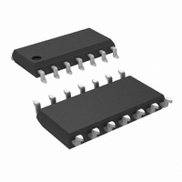
LM324MX/NOPB National Semiconductor, LM324MX/NOPB Datasheet - Page 8

LM324MX/NOPB
Manufacturer Part Number
LM324MX/NOPB
Description
IC OP AMP QUAD LOW POWER 14-SOIC
Manufacturer
National Semiconductor
Specifications of LM324MX/NOPB
Amplifier Type
General Purpose
Number Of Circuits
4
Slew Rate
0.5 V/µs
Gain Bandwidth Product
1MHz
Current - Input Bias
45nA
Voltage - Input Offset
2000µV
Current - Supply
1.5mA
Current - Output / Channel
40mA
Voltage - Supply, Single/dual (±)
3 V ~ 32 V, ±1.5 V ~ 16 V
Operating Temperature
0°C ~ 70°C
Mounting Type
Surface Mount
Package / Case
14-SOIC (3.9mm Width), 14-SOL
Bandwidth
1 MHz
Channel Separation
-120
Common Mode Rejection Ratio
85
Current, Input Bias
45 nA
Current, Input Offset
5 nA
Current, Output
40 mA
Current, Supply
0.7 mA
Number Of Amplifiers
Quad
Package Type
SO-14
Power Dissipation
800 mW
Temperature, Operating, Range
0 to +70 °C
Voltage, Gain
100 V/mV
Voltage, Input
-0.3 to +32 V
Voltage, Offset
2 mV
Voltage, Output, High
28 V
Voltage, Output, Low
5 mV
Voltage, Supply
5 V
Leaded Process Compatible
Yes
Rohs Compliant
Yes
Peak Reflow Compatible (260 C)
Yes
Lead Free Status / RoHS Status
Lead free / RoHS Compliant
Output Type
-
-3db Bandwidth
-
Lead Free Status / Rohs Status
RoHS Compliant part
Electrostatic Device
Other names
LM324MX
LM324MX
LM324MXTR
LM324MX
LM324MXTR
Available stocks
Company
Part Number
Manufacturer
Quantity
Price
Company:
Part Number:
LM324MX/NOPB
Manufacturer:
Texas Instruments
Quantity:
4 000
Part Number:
LM324MX/NOPB
Manufacturer:
TI/德州仪器
Quantity:
20 000
www.national.com
Typical Performance Characteristics
Application Hints
The LM124 series are op amps which operate with only a
single power supply voltage, have true-differential inputs,
and remain in the linear mode with an input common-mode
voltage of 0 V
of power supply voltage with little change in performance
characteristics. At 25˚C amplifier operation is possible down
to a minimum supply voltage of 2.3 V
The pinouts of the package have been designed to simplify
PC board layouts. Inverting inputs are adjacent to outputs for
all of the amplifiers and the outputs have also been placed at
the corners of the package (pins 1, 7, 8, and 14).
Precautions should be taken to insure that the power supply
for the integrated circuit never becomes reversed in polarity
or that the unit is not inadvertently installed backwards in a
test socket as an unlimited current surge through the result-
ing forward diode within the IC could cause fusing of the
internal conductors and result in a destroyed unit.
Large differential input voltages can be easily accommo-
dated and, as input differential voltage protection diodes are
not needed, no large input currents result from large differ-
ential input voltages. The differential input voltage may be
larger than V
DC
+
Input Current (LM2902 only)
. These amplifiers operate over a wide range
without damaging the device. Protection
Output Characteristics
Current Sinking
DC
.
00929944
00929946
8
(Continued)
should be provided to prevent the input voltages from going
negative more than −0.3 V
with a resistor to the IC input terminal can be used.
To reduce the power supply drain, the amplifiers have a
class A output stage for small signal levels which converts to
class B in a large signal mode. This allows the amplifiers to
both source and sink large output currents. Therefore both
NPN and PNP external current boost transistors can be used
to extend the power capability of the basic amplifiers. The
output voltage needs to raise approximately 1 diode drop
above ground to bias the on-chip vertical PNP transistor for
output current sinking applications.
For ac applications, where the load is capacitively coupled to
the output of the amplifier, a resistor should be used, from
the output of the amplifier to ground to increase the class A
bias current and prevent crossover distortion.
Where the load is directly coupled, as in dc applications,
there is no crossover distortion.
Capacitive loads which are applied directly to the output of
the amplifier reduce the loop stability margin. Values of
50 pF can be accommodated using the worst-case non-
inverting unity gain connection. Large closed loop gains or
resistive isolation should be used if larger load capacitance
must be driven by the amplifier.
Voltage Gain (LM2902 only)
Current Limiting
DC
(at 25˚C). An input clamp diode
00929945
00929947


