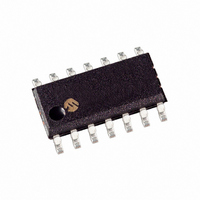
MCP6284-E/SL Microchip Technology, MCP6284-E/SL Datasheet - Page 12

MCP6284-E/SL
Manufacturer Part Number
MCP6284-E/SL
Description
IC OPAMP 2.2V QUAD R-R 14SOIC
Manufacturer
Microchip Technology
Specifications of MCP6284-E/SL
Slew Rate
2.5 V/µs
Package / Case
14-SOIC (3.9mm Width), 14-SOL
Amplifier Type
General Purpose
Number Of Circuits
4
Output Type
Rail-to-Rail
Gain Bandwidth Product
5MHz
Current - Input Bias
1pA
Voltage - Input Offset
3000µV
Current - Supply
450µA
Current - Output / Channel
25mA
Voltage - Supply, Single/dual (±)
2.2 V ~ 6 V
Operating Temperature
-40°C ~ 125°C
Mounting Type
Surface Mount
Number Of Channels
4
Common Mode Rejection Ratio (min)
70 dB
Input Offset Voltage
3 mV
Input Bias Current (max)
1 pA
Operating Supply Voltage
3 V, 5 V
Maximum Operating Temperature
+ 125 C
Minimum Operating Temperature
- 40 C
Mounting Style
SMD/SMT
Shutdown
No
Supply Voltage (max)
5.5 V
Supply Voltage (min)
2.2 V
Technology
CMOS
Voltage Gain Db
110 dB
Lead Free Status / RoHS Status
Lead free / RoHS Compliant
-3db Bandwidth
-
Lead Free Status / Rohs Status
Lead free / RoHS Compliant
Available stocks
Company
Part Number
Manufacturer
Quantity
Price
Company:
Part Number:
MCP6284-E/SL
Manufacturer:
MICROCHIP
Quantity:
12 000
Part Number:
MCP6284-E/SL
Manufacturer:
MICROCHIP/微芯
Quantity:
20 000
MCP6281/2/3/4/5
FIGURE 4-4:
for Capacitive Loads.
After selecting R
resulting frequency response peaking and step
response overshoot. Modify R
response is reasonable. Bench evaluation and simula-
tions with the MCP6281/2/3/4/5 SPICE macro model
are helpful.
4.4
The MCP6283 and MCP6285 are single and dual op
amps with Chip Select (CS), respectively. When CS is
pulled high, the supply current drops to 0.7 µA (typ) and
flows through the CS pin to V
the amplifier output is put into a high-impedance state.
By pulling CS low, the amplifier is enabled. If the CS pin
is left floating, the amplifier may not operate properly.
Figure 1-1 shows the output voltage and supply current
response to a CS pulse.
4.5
The MCP6285 is a dual op amp with Chip Select (CS).
The Chip Select input is available on what would be the
non-inverting input of a standard dual op amp (pin 5).
This pin is available because the output of op amp A
connects to the non-inverting input of op amp B, as
shown in Figure 4-5. The Chip Select input, which can
be connected to a microcontroller I/O line, puts the
device in Low-power mode. Refer to Section 4.4
“MCP6283/5 Chip Select (CS)”.
DS21811D-page 12
1,000
100
10
MCP628X Chip Select (CS)
Cascaded Dual Op Amps
(MCP6285)
10
Normalized Load Capacitance; C
ISO
for your circuit, double-check the
100
Recommended R
G
G
G
SS
N
N
N
= 1 V/V
= 2 V/V
ISO
. When this happens,
4 V/V
1,000
's value until the
L
/G
ISO
N
(pF)
Values
10,000
FIGURE 4-5:
The output of op amp A is loaded by the input imped-
ance of op amp B, which is typically 10
specified in the DC specification table (Refer to
Section 4.3 “Capacitive Loads” for further details
regarding capacitive loads).
The common mode input range of these op amps is
specified in the data sheet as V
V
is limited to V
10 k load), the non-inverting input range of op amp B
is limited to the common mode input range of
V
4.6
With this family of operational amplifiers, the power
supply pin (V
bypass capacitor (i.e., 0.01 µF to 0.1 µF) within 2 mm
for good, high-frequency performance. It also needs a
bulk capacitor (i.e., 1 µF or larger) within 100 mm to
provide large, slow currents. This bulk capacitor can be
shared with other analog parts.
4.7
In applications where low input bias current is critical,
Printed Circuit Board (PCB) surface-leakage effects
need to be considered. Surface leakage is caused by
humidity, dust or other contamination on the board.
Under low humidity conditions, a typical resistance
between nearby traces is 10
cause 5 pA of current to flow, which is greater than the
MCP6281/2/3/4/5 family’s bias current at 25°C (1 pA,
typ.).
The easiest way to reduce surface leakage is to use a
guard ring around sensitive pins (or traces). The guard
ring is biased at the same voltage as the sensitive pin.
An example of this type of layout is shown in
Figure 4-6.
V
V
DD
SS
INA
INA
+ 20 mV and V
+ 300 mV. However, since the output of op amp A
+
–
2
3
Supply Bypass
PCB Surface Leakage
DD
OL
A
V
for single-supply) should have a local
and V
OUTA
DD
1
MCP6285
/V
Cascaded Gain Amplifier.
OH
– 20 mV.
INB
2004 Microchip Technology Inc.
CS
(20 mV from the rails with a
+
12
5
V
. A 5V difference would
INB
6
–
SS
B
– 300 mV and
13
7
|| 6 pF, as
V
OUTB


