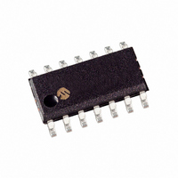
MCP6284-E/SL Microchip Technology, MCP6284-E/SL Datasheet - Page 14

MCP6284-E/SL
Manufacturer Part Number
MCP6284-E/SL
Description
IC OPAMP 2.2V QUAD R-R 14SOIC
Manufacturer
Microchip Technology
Specifications of MCP6284-E/SL
Slew Rate
2.5 V/µs
Package / Case
14-SOIC (3.9mm Width), 14-SOL
Amplifier Type
General Purpose
Number Of Circuits
4
Output Type
Rail-to-Rail
Gain Bandwidth Product
5MHz
Current - Input Bias
1pA
Voltage - Input Offset
3000µV
Current - Supply
450µA
Current - Output / Channel
25mA
Voltage - Supply, Single/dual (±)
2.2 V ~ 6 V
Operating Temperature
-40°C ~ 125°C
Mounting Type
Surface Mount
Number Of Channels
4
Common Mode Rejection Ratio (min)
70 dB
Input Offset Voltage
3 mV
Input Bias Current (max)
1 pA
Operating Supply Voltage
3 V, 5 V
Maximum Operating Temperature
+ 125 C
Minimum Operating Temperature
- 40 C
Mounting Style
SMD/SMT
Shutdown
No
Supply Voltage (max)
5.5 V
Supply Voltage (min)
2.2 V
Technology
CMOS
Voltage Gain Db
110 dB
Lead Free Status / RoHS Status
Lead free / RoHS Compliant
-3db Bandwidth
-
Lead Free Status / Rohs Status
Lead free / RoHS Compliant
Available stocks
Company
Part Number
Manufacturer
Quantity
Price
Company:
Part Number:
MCP6284-E/SL
Manufacturer:
MICROCHIP
Quantity:
12 000
Part Number:
MCP6284-E/SL
Manufacturer:
MICROCHIP/微芯
Quantity:
20 000
MCP6281/2/3/4/5
4.8.3
The MCP6285 provides the flexibility of Low-power
mode for dual op amps in an 8-pin package. The
MCP6285 eliminates the added cost and space in
battery-powered applications by using two single op
amps with Chip Select lines or a 10-pin device with one
Chip Select line for both op amps. Since the two op
amps are internally cascaded, this device cannot be
used in circuits that require active or passive elements
between the two op amps. However, there are several
applications where this op amp configuration with
Chip Select line becomes suitable. The circuits below
show possible applications for this device.
4.8.3.1
With the cascaded op amp configuration, op amp B can
be used to isolate the load from op amp A. In applica-
tions where op amp A is driving capacitive or low resis-
tance loads in the feedback loop (such as an integrator
circuit or filter circuit), the op amp may not have
sufficient source current to drive the load. In this case,
op amp B can be used as a buffer.
FIGURE 4-9:
Buffer.
4.8.3.2
Figure 4-10 shows a cascaded gain circuit configura-
tion with Chip Select. Op amps A and B are configured
in a non-inverting amplifier configuration. In this
configuration, it is important to note that the input offset
voltage of op amp A is amplified by the gain of
op amp A and B, as shown below:
Therefore, it is recommended to set most of the gain
with op amp A and use op amp B with relatively small
gain (e.g., a unity-gain buffer).
DS21811D-page 14
Where:
V
V
V
OUT
OSA
OSB
G
G
A
B
=
CASCADED OP AMP
APPLICATIONS
A
= op amp A gain
= op amp B gain
= op amp A input offset voltage
= op amp B input offset voltage
Load Isolation
Cascaded Gain
V
IN
G
A
MCP6285
G
B
Isolating the Load with a
CS
+
V
OSA
G
A
G
B
B
+
V
OSB
Load
G
V
B
OUTB
FIGURE 4-10:
Configuration.
4.8.3.3
Figure 4-11 shows op amp A configured as a difference
amplifier with Chip Select. In this configuration, it is
recommended to use well-matched resistors (e.g.,
0.1%) to increase the Common Mode Rejection Ratio
(CMRR). Op amp B can be used to provide additional
gain and isolate the load from the difference amplifier.
FIGURE 4-11:
V
V
IN2
IN1
R
V
4
IN
R
R
R
2
2
1
Difference Amplifier
A
R
3
R
A
1
MCP6285
Cascaded Gain Circuit
Difference Amplifier Circuit.
2004 Microchip Technology Inc.
MCP6285
CS
CS
R
R
4
2
R
R
B
1
B
3
V
V
OUT
OUT


