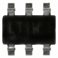
LT1784CS6#TRMPBF Linear Technology, LT1784CS6#TRMPBF Datasheet - Page 5

LT1784CS6#TRMPBF
Manufacturer Part Number
LT1784CS6#TRMPBF
Description
IC OPAMP R-R IN/OUT SOT23-6
Manufacturer
Linear Technology
Series
Over-The-Top®r
Datasheet
1.LT1784CS6TRM.pdf
(12 pages)
Specifications of LT1784CS6#TRMPBF
Amplifier Type
General Purpose
Number Of Circuits
1
Output Type
Rail-to-Rail
Slew Rate
2.2 V/µs
Gain Bandwidth Product
2.6MHz
Current - Input Bias
250nA
Voltage - Input Offset
1600µV
Current - Supply
750µA
Current - Output / Channel
27mA
Voltage - Supply, Single/dual (±)
2.5 V ~ 18 V, ±1.25 V ~ 9 V
Operating Temperature
0°C ~ 70°C
Mounting Type
Surface Mount
Package / Case
SOT-23-6
Lead Free Status / RoHS Status
Lead free / RoHS Compliant
-3db Bandwidth
-
Other names
LT1784CS6#TRMPBFTR
Available stocks
Company
Part Number
Manufacturer
Quantity
Price
ELECTRICAL CHARACTERISTICS
temperature range, otherwise specifi cations are at T
pulse power tested unless otherwise specifi ed.
SYMBOL
V
V
t
t
GBW
SR
FPBW
t
Note 1: Stresses beyond those listed under Absolute Maximum Ratings
may cause permanent damage to the device. Exposure to any Absolute
Maximum Rating condition for extended periods may affect device
reliability and lifetime.
Note 2: A heat sink may be required to keep the junction temperature
below absolute maximum.
Note 3: V
V
Note 4: V
V
Note 5: Guaranteed by correlation to slew rate at V
V
TYPICAL PERFORMANCE CHARACTERISTICS
ON
OFF
S
IL
IH
S
S
S
= ±5V or V
= ±5V or V
= 5V and V
700
650
600
550
500
450
400
350
300
2
Supply Current vs Supply Voltage
S
S
= 5V limits are guaranteed by correlation to V
= 3V limits are guaranteed by correlation to V
PARAMETER
SHDN Pin Input Low Voltage
SHDN Pin Input High Voltage
Turn-On Time
Turn-Off Time
Gain Bandwidth Product
Slew Rate
Full-Power Bandwidth (Note 9)
Settling Time
T
4
A
S
S
S
= 125°C
= ±9V tests.
= ±9V tests.
= ±5V tests.
6
SUPPLY VOLTAGE (V)
8
T
A
10
= 25°C
12
T
A
= –55°C
14
16
1784 G01
18
S
= ±5V, and GBW at
CONDITIONS
V
V
V
V
f = 5kHz
0°C ≤ T
–40°C ≤ T
A
0°C ≤ T
–40°C ≤ T
V
V
–100
–200
–300
–400
S
S
PIN5
PIN5
V
OUT
S
S
S
400
300
200
100
= –1, R
= ±5V (Note 8)
= ±5V (Note 8)
= 5V, ΔV
= 3V and
= 5V and
0
A
= 8V
1
= 0V to –5V, R
= –5V to 0V, R
Minimum Supply Voltage
T
= 25°C. V
A
A
A
≤ 70°C
≤ 70°C
= 125°C
A
A
P-P
L
OUT
≤ 85°C
≤ 85°C
= ∞, V
The
TOTAL SUPPLY VOLTAGE (V)
= 4V to 0.1%, A
2
l
S
O
L
L
denotes the specifi cations which apply over the specifi ed
= ±5V, V
= ±4V, Measured at V
= 10k (Note 8)
= 10k (Note 8)
T
A
= 25°C
3
Note 6: This specifi cation implies a typical input offset voltage of 5.7mV at
V
Note 7: This parameter is not 100% tested.
Note 8: Specifi cations apply to 6-lead SOT-23 with shutdown.
Note 9: Full-power bandwidth is calculated from the slew rate.
FPBW = SR/2πV
Note 10: The LT1784C is guaranteed functional over the operating
temperature range –40°C to 85°C.
Note 11: The LT1784C is guaranteed to meet specifi ed performance from
0°C to 70°C. The LT1784C is designed, characterized and expected to
meet specifi ed performance from –40°C to 85°C but is not tested or QA
sampled at these temperatures. LT1784I is guaranteed to meet specifi ed
performance from –40°C to 85°C.
CM
T
CM
= 18V and a maximum input offset voltage of 18mV at V
A
V
= –55°C
= 0V, V
= 1
4
1784 G02
OUT
O
P
.
= ±2V
5
= 0V, for the 6-lead part V
l
l
l
l
l
l
l
l
5
4
3
2
1
0
–10
Output Voltage
vs Large Input Voltage
1.55
1.30
1.20
MIN
V
1.3
1.2
1.1
–3
S
= 5V, 0V
–6
–2
TYP
2.2
2.6
2.2
3.4
18
94
PIN5
2
V
IN
(V)
= V
V
6
IN
LT1784
MAX
–4.7
–
,
+
–
10
CM
5V
= 18V.
14
UNITS
1784 G03
1784fa
5
MHz
MHz
MHz
V/μs
V/μs
V/μs
kHz
18
μs
μs
μs
V
V


