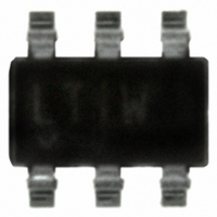
LT1784CS6#TRMPBF Linear Technology, LT1784CS6#TRMPBF Datasheet - Page 9

LT1784CS6#TRMPBF
Manufacturer Part Number
LT1784CS6#TRMPBF
Description
IC OPAMP R-R IN/OUT SOT23-6
Manufacturer
Linear Technology
Series
Over-The-Top®r
Datasheet
1.LT1784CS6TRM.pdf
(12 pages)
Specifications of LT1784CS6#TRMPBF
Amplifier Type
General Purpose
Number Of Circuits
1
Output Type
Rail-to-Rail
Slew Rate
2.2 V/µs
Gain Bandwidth Product
2.6MHz
Current - Input Bias
250nA
Voltage - Input Offset
1600µV
Current - Supply
750µA
Current - Output / Channel
27mA
Voltage - Supply, Single/dual (±)
2.5 V ~ 18 V, ±1.25 V ~ 9 V
Operating Temperature
0°C ~ 70°C
Mounting Type
Surface Mount
Package / Case
SOT-23-6
Lead Free Status / RoHS Status
Lead free / RoHS Compliant
-3db Bandwidth
-
Other names
LT1784CS6#TRMPBFTR
Available stocks
Company
Part Number
Manufacturer
Quantity
Price
APPLICATIONS INFORMATION
Supply Voltage
The positive supply pin of the LT1784 should be bypassed
with a small capacitor (typically 0.1μF) within an inch of
the pin. When driving heavy loads, and additional 4.7μF
electrolytic capacitor should be used. When using split
supplies the same is true for the negative supply pin.
The LT1784 is protected against reverse battery voltages
up to 18V. In the event a reverse battery condition occurs
the supply current is less than 1nA.
Inputs
The LT1784 has two input stages, NPN and PNP (see the
Simplifi ed Schematic), resulting in three distinct operating
regions as shown in the “Input Bias Current vs Common
Mode” Typical Performance Characteristic curve.
For input voltages about 1V or more below V
input stage is active and the input bias current is typically
–250nA. When the input common mode voltage is within
0.6V of the positive rail, the NPN stage is operating and
the input bias current is typically 500nA. Increases in
temperature will cause the voltage at which operation
switches from the PNP input stage to the NPN input stage
to move towards V
stage is untrimmed and is typically 3mV.
A Schottky diode in the collector of the input transistors,
along with special geometries for these NPN transistors,
allow the LT1784 to operate with either or both of its inputs
above V
tors is fully saturated and the input bias current is typically
200μA at room temperature. The input offset voltage is
typically 3mV when operating above V
operate with inputs 18V above V
The inputs are protected against excursions as much as
10V below V
input and a diode from the input to the negative supply.
The input stage of the LT1784 incorporates phase reversal
protection to prevent the output from phase reversing for
inputs up to 9V below V
between the inputs and the maximum differential input
voltage is 18V.
+
. At about 0.3V above V
–
by an internal 1k resistor in series with each
+
. The input offset voltage of the NPN
–
. There are no clamping diodes
+
–
, the NPN input transis-
regardless of V
+
. The LT1784 will
+
, the PNP
+
.
Output
The output of the LT1784 can swing to within 80mV of the
positive rail and within 4mV of the negative rail with no
load. When monitoring input voltages within 80mV of the
positive rail or within 4mV of the negative rail, gain should
be taken to keep the output from clipping. The LT1784
can typically sink and source over 25mA at ±5V supplies,
sourcing current is reduced to 7.5mA at 3V total supplies
as noted in the Electrical Characteristics section.
The LT1784 is internally compensated to drive at least
400pF of capacitance under any output loading condi-
tions. A 0.22μF capacitor in series with a 150Ω resistor
between the output and ground will compensate these
amplifi ers for larger capacitive loads, up to 10,000pF at
all output currents.
Distortion
There are two main contributors to distortion in op amps:
output crossover distortion as the output transitions from
sourcing to sinking current, and distortion caused by non-
linear common mode rejection. If the op amp is operating
inverting, there is no common mode induced distortion.
If the op amp is operating in the PNP input stage (input
not within 1V of V
95dB. When the LT1784 switches between input stages,
there is signifi cant nonlinearity in the CMRR. Lower load
resistance increases the output crossover distortion but
has no effect on the input stage transition distortion. For
lowest distortion, the LT1784 should be operated single
supply, with the output always sourcing current and with
the input voltage swing between ground and (V
Typical Performance Characteristics curve, “Total Harmonic
Distortion + Noise vs Output Voltage Amplitude.”
Gain
The open-loop gain is almost independent of load when
the output is sourcing current. This optimizes performance
in single supply applications where the load is returned
to ground. The Typical Performance Characteric curve
“Open-Loop Gain” for various loads shows the details.
+
), the CMRR is very good, typically
LT1784
+
– 1V). See
1784fa
9


