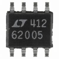
LT6200CS8-5#TR Linear Technology, LT6200CS8-5#TR Datasheet - Page 21

LT6200CS8-5#TR
Manufacturer Part Number
LT6200CS8-5#TR
Description
IC OP AMP 800MHZ R-R I/O 8-SOIC
Manufacturer
Linear Technology
Datasheet
1.LT6200CS6TRMPBF.pdf
(26 pages)
Specifications of LT6200CS8-5#TR
Amplifier Type
Buffer
Number Of Circuits
1
Output Type
Rail-to-Rail
Slew Rate
250 V/µs
Gain Bandwidth Product
800MHz
Current - Input Bias
23µA
Voltage - Input Offset
2500µV
Current - Supply
20mA
Current - Output / Channel
90mA
Voltage - Supply, Single/dual (±)
2.5 V ~ 12.6 V, ±1.25 V ~ 6.3 V
Operating Temperature
0°C ~ 70°C
Mounting Type
Surface Mount
Package / Case
8-SOIC (3.9mm Width)
Lead Free Status / RoHS Status
Contains lead / RoHS non-compliant
-3db Bandwidth
-
Available stocks
Company
Part Number
Manufacturer
Quantity
Price
APPLICATIONS INFORMATION
Figure 2 shows the input and output waveforms of the
LT6200 driven into clipping while connected in a gain of
A
at ±35mA, and the output transistors supply this generator
current through the protection diodes.
ESD
The LT6200 has reverse-biased ESD protection diodes on
all inputs and outputs, as shown in Figure 1. If these pins
are forced beyond either supply, unlimited current will fl ow
through these diodes. If the current is transient and limited
to 30mA or less, no damage to the device will occur.
Noise
The noise voltage of the LT6200 is equivalent to that of
a 56Ω resistor—and for the lowest possible noise, it is
desirable to keep the source and feedback resistance
at or below this value (i.e., R
R
e
tance value the amplifi er dominates the noise, but in the
resistance region between 56Ω and approximately 6kΩ,
the noise is dominated by the resistor thermal noise. As
the total resistance is further increased, beyond 6k, the
noise current multiplied by the total resistance eventually
dominates the noise.
For a complete discussion of amplifi er noise, see the
LT1028 data sheet.
n
V
S
0V
= 1. In this photo, the input signal generator is clipping
= √(0.95nV)
+ R
Figure 2. V
G
//R
FB
= 56Ω the total noise of the amplifi er is:
2
S
+ (0.95nV)
= ±2.5V, A
V
2
= 1 with Large Overdrive
= 1.35nV. Below this resis-
S
+ R
G
//R
FB
≤ 56Ω). With
6200 F02
V
2.5V
V
–2.5V
CC
EE
Power Dissipation
The LT6200 combines high speed with large output cur-
rent in a small package, so there is a need to ensure that
the die’s junction temperature does not exceed 150°C.
The LT6200 is housed in a 6-lead TSOT-23 package. The
package has the V
enhance the thermal conductance when connecting to a
ground plane or a large metal trace. Metal trace and plated
through-holes can be used to spread the heat generated by
the device to the backside of the PC board. For example,
on a 3/32" FR-4 board with 2oz copper, a total of 270mm
connects to Pin 2 of the LT6200 (in a TSOT-23 package)
bringing the thermal resistance, θ
Without an extra metal trace beside the power line con-
necting to the V
resistance will be around 200°C/W. More information on
thermal resistance with various metal areas connecting
to the V
Table 1. LT6200 6-Lead TSOT-23 Package
Device is mounted on topside.
Junction temperature T
temperature T
The power dissipation in the IC is the function of the supply
voltage, output voltage and the load resistance. For a given
supply voltage, the worst-case power dissipation P
occurs at the maximum quiescent supply current and at
the output voltage which is half of either supply voltage
(or the maximum swing if it is less than half the supply
voltage). P
Example: An LT6200 in TSOT-23 mounted on a 2500mm
area of PC board without any extra heat spreading plane
connected to its V
TOPSIDE (mm
T
P
COPPER AREA
J
D(MAX)
= T
270
100
20
–
0
A
pin is provided in Table 1.
+ (P
D(MAX)
= (V
2
A
)
D
S
and power dissipation P
• θ
–
• I
pin to provide a heat sink, the thermal
is given by:
–
JA
S(MAX)
supply pin fused to the lead frame to
BOARD AREA
–
)
LT6200-10/LT6201
pin has a thermal resistance of
(mm
LT6200/LT6200-5
2500
2500
2500
2500
J
is calculated from the ambient
) + (V
2
)
S
/2)
JA
(JUNCTION-TO-AMBIENT)
2
THERMAL RESISTANCE
, to about 135°C/W.
/R
L
D
135ºC/W
145ºC/W
160ºC/W
200ºC/W
as follows:
21
D(MAX)
62001fd
2
2


