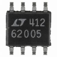
LT6200CS8-5#TR Linear Technology, LT6200CS8-5#TR Datasheet - Page 22

LT6200CS8-5#TR
Manufacturer Part Number
LT6200CS8-5#TR
Description
IC OP AMP 800MHZ R-R I/O 8-SOIC
Manufacturer
Linear Technology
Datasheet
1.LT6200CS6TRMPBF.pdf
(26 pages)
Specifications of LT6200CS8-5#TR
Amplifier Type
Buffer
Number Of Circuits
1
Output Type
Rail-to-Rail
Slew Rate
250 V/µs
Gain Bandwidth Product
800MHz
Current - Input Bias
23µA
Voltage - Input Offset
2500µV
Current - Supply
20mA
Current - Output / Channel
90mA
Voltage - Supply, Single/dual (±)
2.5 V ~ 12.6 V, ±1.25 V ~ 6.3 V
Operating Temperature
0°C ~ 70°C
Mounting Type
Surface Mount
Package / Case
8-SOIC (3.9mm Width)
Lead Free Status / RoHS Status
Contains lead / RoHS non-compliant
-3db Bandwidth
-
Available stocks
Company
Part Number
Manufacturer
Quantity
Price
LT6200/LT6200-5
LT6200-10/LT6201
APPLICATIONS INFORMATION
200°C/W, θ
loads, the worst-case power dissipation is given by:
The maximum ambient temperature that the part is
allowed to operate is:
To operate the device at a higher ambient temperature,
connect more metal area to the V
resistance of the package, as indicated in Table 1.
DD Package Heat Sinking
The underside of the DD package has exposed metal
(4mm
This provides for the direct transfer of heat from the die
junction to printed circuit board metal to help control the
maximum operating junction temperature. The dual-in-line
pin arrangement allows for extended metal beyond the
ends of the package on the topside (component side) of
22
P
T
A
D(MAX)
= T
= 150°C – (0.355W • 200°C/W) = 79°C
2
) from the lead frame where the die is attached.
J
– (P
= (10 • 23mA) + (2.5)
= 0.23 + 0.125 = 0.355W
JA
. Operating on ± 5V supplies driving 50Ω
D(MAX)
• 200°C/W)
–
pin to reduce the thermal
2
/50
a PCB. Table 2 summarizes the thermal resistance from
the die junction-to-ambient that can be obtained using
various amounts of topside metal (2oz copper) area. On
multilayer boards, further reductions can be obtained using
additional metal on inner PCB layers connected through
vias beneath the package.
Table 2. LT6200 8-Lead DD Package
The LT6200 amplifi er family has thermal shutdown to
protect the part from excessive junction temperature.
The amplifi er will shut down to approximately 1.2mA
supply current per amplifi er if the maximum temperature
is exceeded. The LT6200 will remain off until the junction
temperature reduces to about 135°C, at which point the
amplifi er will return to normal operation.
TOPSIDE (mm
COPPER AREA
130
16
32
64
4
2
)
(JUNCTION-TO-AMBIENT)
THERMAL RESISTANCE
160ºC/W
135ºC/W
110ºC/W
95ºC/W
70ºC/W
62001fd


