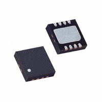
LT1816IDD Linear Technology, LT1816IDD Datasheet - Page 8

LT1816IDD
Manufacturer Part Number
LT1816IDD
Description
IC OP AMP 220MHZ DUAL LP 8-DFN
Manufacturer
Linear Technology
Datasheet
1.LT1817CGNPBF.pdf
(20 pages)
Specifications of LT1816IDD
Amplifier Type
Voltage Feedback
Number Of Circuits
2
Slew Rate
1500 V/µs
Gain Bandwidth Product
220MHz
-3db Bandwidth
350MHz
Current - Input Bias
2µA
Voltage - Input Offset
200µV
Current - Supply
6.5mA
Current - Output / Channel
80mA
Voltage - Supply, Single/dual (±)
2.5 V ~ 11 V, ±1.25 V ~ 5.5 V
Operating Temperature
-40°C ~ 85°C
Mounting Type
Surface Mount
Package / Case
8-DFN
Lead Free Status / RoHS Status
Contains lead / RoHS non-compliant
Output Type
-
Available stocks
Company
Part Number
Manufacturer
Quantity
Price
Company:
Part Number:
LT1816IDD
Manufacturer:
LT
Quantity:
10 000
Part Number:
LT1816IDD#PBF
Manufacturer:
LINEAR/凌特
Quantity:
20 000
Company:
Part Number:
LT1816IDD/C
Manufacturer:
LT
Quantity:
213
LT1815/LT1816/LT1817
ELECTRICAL CHARACTERISTICS
Note 3: A heat sink may be required to keep the junction temperature
below absolute maximum when the output is shorted indefi nitely.
Note 4: Input offset voltage is pulse tested and is exclusive of warm-up
drift.
Note 5: Slew rate is measured between ±2V at the output with ±3V input
for ±5V supplies and 2V
supplies.
Note 6: Full-power bandwidth is calculated from the slew rate:
Note 7: This parameter is not 100% tested.
Note 8: The LT1815C/LT1816C/LT1817C are guaranteed to meet specifi ed
performance from 0°C to 70°C and are designed, characterized and
TYPICAL PERFORMANCE CHARACTERISTICS
8
–0.4
–0.8
–1.2
–1.6
–2.0
–2.4
–2.8
FPBW = SR/2πV
12
10
6
0
8
4
2
0
–50
–50 –25
Supply Current vs Temperature
Input Bias Current vs Temperature
PER AMPLIFIER
–25
V
0
0
S
TEMPERATURE (°C)
TEMPERATURE (°C)
P
= ±5V
25
25
P-P
V
V
S
S
at the output with a 3V
= ±2.5V
50
= ±5V
50
V
S
= ±2.5V
75
75
100
100
181567 G04
181567 G01
125
125
P-P
input for single 5V
–0.5
–1.0
–1.5
–2.0
100
2.0
1.5
1.0
0.5
10
V
V
1
+
–
10
0
Input Common Mode Range
vs Supply Voltage
Input Noise Spectral Density
T
ΔV
A
OS
= 25°C
1
< 1mV
100
SUPPLY VOLTAGE (±V)
2
FREQUENCY (Hz)
3
1k
e
i
n
n
expected to meet the extended temperature limits, but are not tested at
–40°C and 85°C. The LT1815I/LT1816I/LT1817I are guaranteed to meet the
extended temperature limits.
Note 9: Thermal resistance (θ
metal connected to the package. The specifi ed values are for short
traces connected to the leads. If desired, the thermal resistance can be
substantially reduced by connecting Pin 2 of the TSOT-23, Pin 4 of the
SO-8 and MS8, Pin 5 of the MS10 or the underside metal of the DD
package to a large metal area.
Note 10: A resistor of 40k or less is required between the I
of the LT1815S6 and the LT1816AMS. See the Applications Information
section for information on selecting a suitable resistor.
4
5
10k
T
V
A
R
A
S
V
S
= 25°C
= ±5V
= 101
= 10k
6
181567 G02
181567 G05
100k
7
1
10
0.1
JA
75.0
70.0
60.0
72.5
67.5
65.0
62.5
) varies with the amount of PC board
–3
–4
–1
–2
0
–5.0
100
Input Bias Current
vs Common Mode Voltage
Open-Loop Gain vs Resistive Load
T
V
T
A
S
A
= 25°C
= ±5V
= 25°C
INPUT COMMON MODE VOLTAGE (V)
–2.5
LOAD RESISTANCE (Ω)
1k
0
V
V
S
S
= ±5V
= ±2.5V
SET
and V
2.5
181567fb
–
181567 G03
181567 G06
pins
10k
5.0


