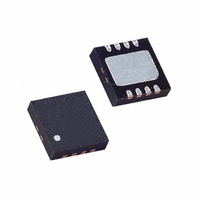
LT1816IDD Linear Technology, LT1816IDD Datasheet

LT1816IDD
Specifications of LT1816IDD
Available stocks
Related parts for LT1816IDD
LT1816IDD Summary of contents
Page 1
... TSOT-23, SO, MSOP , SSOP and leadless DFN packages. L, LT, LTC, LTM, Linear Technology and the Linear logo are registered trademarks of Linear Technology Corporation. ThinSOT is a trademark of Linear Technology Corporation. All other trademarks are the property of their respective owners. ...
Page 2
LT1815/LT1816/LT1817 ABSOLUTE MAXIMUM RATINGS + – Total Supply Voltage ( ............................. 12.6V Differential Input Voltage (Transient Only, Note 2) ........................................... ±6V Input Voltage ........................................................... ±V Output Short-Circuit Duration (Note 3) .......... Indefi nite Operating Temperature Range .................–40°C ...
Page 3
... ORDER INFORMATION LEAD FREE FINISH TAPE AND REEL LT1815CS5#PBF LT1815CS5#TRPBF LT1815IS5#PBF LT1815IS5#TRPBF LT1815CS6#PBF LT1815CS6#TRPBF LT1815IS6#PBF LT1815IS6#TRPBF LT1815CS8#PBF LT1815CS8#TRPBF LT1815IS8#PBF LT1815IS8#TRPBF LT1816CDD#PBF LT1816CDD#TRPBF LT1816IDD#PBF LT1816IDD#TRPBF LT1816CMS8#PBF LT1816CMS8#TRPBF LT1816IMS8#PBF LT1816IMS8#TRPBF LT1816ACMS#PBF LT1816ACMS#TRPBF LT1816AIMS#PBF LT1816AIMS#TRPBF LT1816CS8#PBF LT1816CS8#TRPBF LT1816IS8#PBF LT1816IS8#TRPBF LT1817CGN#PBF LT1817CGN#TRPBF LT1817IGN#PBF LT1817IGN#TRPBF LT1817CS#PBF ...
Page 4
LT1815/LT1816/LT1817 ELECTRICAL CHARACTERISTICS temperature range, otherwise specifi cations are at T programmable current option (LT1815S6 or LT1816A), the I otherwise noted. SYMBOL PARAMETER e Input Noise Voltage Density n i Input Noise Current Density n R Input Resistance IN C ...
Page 5
ELECTRICAL CHARACTERISTICS temperature range, otherwise specifi cations are at T programmable current option (LT1815S6 or LT1816A), the I otherwise noted. SYMBOL PARAMETER GBW Gain-Bandwidth Product Gain-Bandwidth Product (Low Power Mode) (Note 10) –3dB BW –3dB Bandwidth Rise ...
Page 6
LT1815/LT1816/LT1817 ELECTRICAL CHARACTERISTICS erature range, otherwise specifi cations are at T programmable current option (LT1815S6 or LT1816A), the I SYMBOL PARAMETER V Input Offset Voltage OS Input Offset Voltage (Low Power Mode) (Note 10) ΔV Input Offset Voltage Drift OS ...
Page 7
ELECTRICAL CHARACTERISTICS erature range, otherwise specifi cations are at T programmable current option (LT1815S6 or LT1816A), the I SYMBOL PARAMETER I Maximum Output Current OUT Maximum Output Current (Low Power Mode) (Note 10) I Output Short-Circuit Current SC SR Slew ...
Page 8
LT1815/LT1816/LT1817 ELECTRICAL CHARACTERISTICS Note 3: A heat sink may be required to keep the junction temperature below absolute maximum when the output is shorted indefi nitely. Note 4: Input offset voltage is pulse tested and is exclusive of warm-up drift. ...
Page 9
TYPICAL PERFORMANCE CHARACTERISTICS Open-Loop Gain vs Temperature 75 ± ± 500Ω L 70.0 67 100Ω L 65.0 62.5 60.0 –50 – 100 125 TEMPERATURE (°C) ...
Page 10
LT1815/LT1816/LT1817 TYPICAL PERFORMANCE CHARACTERISTICS Gain vs Frequency 500Ω 100Ω 25°C A – ± 500Ω ...
Page 11
TYPICAL PERFORMANCE CHARACTERISTICS Slew Rate vs Temperature 2400 + 2000 ±5V S 1600 – ±5V S 1200 + ±2.5V S 800 – ±2. –1 S 400 ...
Page 12
LT1815/LT1816/LT1817 APPLICATIONS INFORMATION Layout and Passive Components As with all high speed amplifi ers, the LT1815/LT1816/ LT1817 require some attention to board layout. A ground plane is recommended and trace lengths should be mini- mized, especially on the negative input ...
Page 13
APPLICATIONS INFORMATION 5V – LT1815S6 – SET R SET –5V 181567 F01 Figure 1. Programming Resistor Between I 250 200 150 R = 100Ω L 100 100 1k R PROGRAMING RESISTOR (Ω) ...
Page 14
LT1815/LT1816/LT1817 SIMPLIFIED SCHEMATIC + V BIAS CONTROL –IN I SET – V LT1815S6/LT1816AMS ONLY TYPICAL APPLICATIONS V IN TRIM R5 FOR GAIN TRIM R1 FOR COMMON MODE REJECTION BW = 2MHz 14 (One Amplifi er) +IN R1 Two Op Amp ...
Page 15
TYPICAL APPLICATIONS PHOTODIODE SIEMENS/ INFINEON SFH213 232Ω Photodiode Transimpedance Amplifi er 1pF 1pF 4.75k 5V – LT1815 + OUTPUT OFFSET ≤1mV TYPICAL –5V BANDWIDTH = 30MHz –5V 10% TO 90% RISE TIME = 22ns OUTPUT NOISE (20MHz BW) ...
Page 16
LT1815/LT1816/LT1817 PACKAGE DESCRIPTION 0.62 MAX 3.85 MAX 2.62 REF RECOMMENDED SOLDER PAD LAYOUT PER IPC CALCULATOR 0.20 BSC DATUM ‘A’ 0.30 – 0.50 REF NOTE: 1. DIMENSIONS ARE IN MILLIMETERS 2. DRAWING NOT TO SCALE 3. DIMENSIONS ARE INCLUSIVE OF ...
Page 17
PACKAGE DESCRIPTION .050 BSC .245 MIN .030 ±.005 TYP RECOMMENDED SOLDER PAD LAYOUT .010 – .020 (0.254 – 0.508) .008 – .010 (0.203 – 0.254) (0.406 – 1.270) NOTE: 1. DIMENSIONS IN (MILLIMETERS) 2. DRAWING NOT TO SCALE 3. THESE ...
Page 18
LT1815/LT1816/LT1817 PACKAGE DESCRIPTION 0.889 0.127 (.035 .005) 5.23 3.20 – 3.45 (.206) (.126 – .136) MIN 0.42 0.038 0.65 (.0165 .0015) (.0256) TYP BSC RECOMMENDED SOLDER PAD LAYOUT NOTE: 1. DIMENSIONS IN MILLIMETER/(INCH) 2. DRAWING NOT TO SCALE 3. DIMENSION ...
Page 19
... MOLD FLASH OR PROTRUSIONS SHALL NOT EXCEED .006" (0.15mm) Information furnished by Linear Technology Corporation is believed to be accurate and reliable. However, no responsibility is assumed for its use. Linear Technology Corporation makes no representa- tion that the interconnection of its circuits as described herein will not infringe on existing patent rights. ...
Page 20
... LT1806/LT1807 Single/Dual 325MHz, 140V/μs Rail-to-Rail I/O Op Amps LT1809/LT1810 Single/Dual 180MHz, 350V/μs Rail-to-Rail I/O Op Amps LT1812/LT1813/LT1814 Single/Dual/Quad 3mA, 100MHz, 750V/μs Op Amps C-Load is a trademark of Linear Technology Corporation. Linear Technology Corporation 20 1630 McCarthy Blvd., Milpitas, CA 95035-7417 (408) 432-1900 FAX: (408) 434-0507 ● ...


