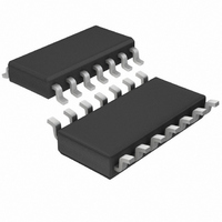
LT6012ACS#TR Linear Technology, LT6012ACS#TR Datasheet

LT6012ACS#TR
Specifications of LT6012ACS#TR
Available stocks
Related parts for LT6012ACS#TR
LT6012ACS#TR Summary of contents
Page 1
... SO-8, MS8 and space saving 3mm × 3mm DFN pack- ages. The LT6012 (quad) is available in SO-14 and 16-pin SSOP packages. , LT, LTC and LTM are registered trademarks of Linear Technology Corporation. SoftSpan is a registered trademark of Linear Technology Corporation. All other trademarks are the property of their respective owners. TM DAC SUPPLY CURRENT ≅ ...
Page 2
LT6011/LT6012 ABSOLUTE AXI U RATI GS + – Total Supply Voltage ( .............................. 40V Differential Input Voltage (Note 2) .......................... 10V Input Voltage .................................................... V Input Current (Note 2) ....................................... ±10mA Output Short-Circuit Duration ...
Page 3
ELECTRICAL CHARACTERISTICS temperature range, otherwise specifications are at T SYMBOL PARAMETER V Input Offset Voltage (Note 8) OS ∆V /∆T Input Offset Voltage Drift (Note Input Offset Current (Note Input Bias Current (Note 8) ...
Page 4
LT6011/LT6012 ELECTRICAL CHARACTERISTICS temperature range, otherwise specifications are at T SYMBOL PARAMETER V Maximum Output Swing OUT + (Positive, Referred to V Maximum Output Swing (Negative, Referred to 0V) I Output Short-Circuit Current (Note Slew Rate ...
Page 5
ELECTRICAL CHARACTERISTICS temperature range, otherwise specifications are at T SYMBOL PARAMETER CONDITIONS V Input Offset Voltage (Note 8) LT6011AS8, LT6012AS LT6011ADD, LT6012AGN T T LT6011S8, LT6012S T T LT6011DD, LT6012GN, LT6011MS8 T T ∆V /∆T Input Offset ...
Page 6
LT6011/LT6012 ELECTRICAL CHARACTERISTICS temperature range, otherwise specifications are at T SYMBOL PARAMETER I Output Short-Circuit Current SC (Note 3) SR Slew Rate GBW Gain Bandwidth Product t Settling Time Rise Time, Fall Time r f ∆V ...
Page 7
W U TYPICAL PERFOR A CE CHARACTERISTICS Distribution of Input Offset Voltage 5V, 0V LT6011S8 25°C LT6012S –90 –70 –50 –30 – ...
Page 8
LT6011/LT6012 W U TYPICAL PERFOR A CE CHARACTERISTICS 0.01Hz to 1Hz Noise = ±15V 25° 100 TIME (SEC) 6011 G10 Output Saturation Voltage vs Load ...
Page 9
W U TYPICAL PERFOR A CE CHARACTERISTICS Settling Time vs Output Step 10 = ±15V – 0.1% 0.01 SETTLING TIME ...
Page 10
LT6011/LT6012 W U TYPICAL PERFOR A CE CHARACTERISTICS Small-Signal Transient Response 20mV/DIV 2µs/DIV 6011 G28 APPLICATIO S I FOR ATIO Preserving Input Precision Preserving the input accuracy of the LT6011/LT6012 re- quires that the ...
Page 11
U U APPLICATIO S I FOR ATIO where e = 14nV/√ 0.1pA/√Hz and impedance at the input, including the source impedance. Capacitive Loads The LT6011/LT6012 can drive capacitive loads up to 500pF in unity ...
Page 12
LT6011/LT6012 PACKAGE DESCRIPTIO 3.5 ±0.05 1.65 ±0.05 2.15 ±0.05 (2 SIDES) 0.25 ± 0.05 0.50 BSC 2.38 ±0.05 (2 SIDES) RECOMMENDED SOLDER PAD PITCH AND DIMENSIONS .050 BSC .245 MIN .030 ± .005 TYP RECOMMENDED SOLDER PAD LAYOUT .010 – ...
Page 13
PACKAGE DESCRIPTIO 5.23 (.206) MIN 0.42 ± 0.038 (.0165 ± .0015) TYP RECOMMENDED SOLDER PAD LAYOUT 0.254 (.010) GAUGE PLANE 0.18 (.007) NOTE: 1. DIMENSIONS IN MILLIMETER/(INCH) 2. DRAWING NOT TO SCALE 3. DIMENSION DOES NOT INCLUDE MOLD FLASH, PROTRUSIONS ...
Page 14
LT6011/LT6012 PACKAGE DESCRIPTIO .050 BSC N .245 MIN .030 ±.005 TYP RECOMMENDED SOLDER PAD LAYOUT .010 – .020 × 45° (0.254 – 0.508) .008 – .010 (0.203 – 0.254) .016 – .050 (0.406 – 1.270) NOTE: INCHES ...
Page 15
... FLASH SHALL NOT EXCEED 0.010" (0.254mm) PER SIDE Information furnished by Linear Technology Corporation is believed to be accurate and reliable. However, no responsibility is assumed for its use. Linear Technology Corporation makes no represen- tation that the interconnection of its circuits as described herein will not infringe on existing patent rights. ...
Page 16
... LT6011-Like Op Amp with 0.04% Matched Resistors 35µV Maximum V ≥ 5 Stable; 1.4MHz GBW A V www.linear.com ● 1/2 LT6011 2 – 49. OUT 49.9k 6 – 7 1/2 LT6011 6011 TA02 Up to 1000pF ; 100pA Maximum I ; Shutdown 0406 REV B • PRINTED IN USA © LINEAR TECHNOLOGY CORPORATION 2003 60112fb ...


