LT6012ACS#TR Linear Technology, LT6012ACS#TR Datasheet - Page 10

LT6012ACS#TR
Manufacturer Part Number
LT6012ACS#TR
Description
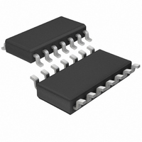
IC OP AMP PREC QUAD R-R 14-SOIC
Manufacturer
Linear Technology
Datasheet
1.LT6011CS8PBF.pdf
(16 pages)
Specifications of LT6012ACS#TR
Amplifier Type
General Purpose
Number Of Circuits
4
Output Type
Rail-to-Rail
Slew Rate
0.11 V/µs
Gain Bandwidth Product
350kHz
Current - Input Bias
20pA
Voltage - Input Offset
30µV
Current - Supply
260µA
Current - Output / Channel
20mA
Voltage - Supply, Single/dual (±)
2.7 V ~ 36 V, ±1.35 V ~ 18 V
Operating Temperature
0°C ~ 70°C
Mounting Type
Surface Mount
Package / Case
14-SOIC (3.9mm Width), 14-SOL
Lead Free Status / RoHS Status
Contains lead / RoHS non-compliant
-3db Bandwidth
-
Available stocks
Company
Part Number
Manufacturer
Quantity
Price
APPLICATIO S I FOR ATIO
20mV/DIV
LT6011/LT6012
Preserving Input Precision
Preserving the input accuracy of the LT6011/LT6012 re-
quires that the applications circuit and PC board layout do
not introduce errors comparable to or greater than the 25µV
typical offset of the amplifiers. Temperature differentials
across the input connections can generate thermocouple
voltages of 10’s of microvolts so the connections to the input
leads should be short, close together and away from heat
dissipating components. Air currents across the board can
also generate temperature differentials.
The extremely low input bias currents (20pA typical) allow
high accuracy to be maintained with high impedance
sources and feedback resistors. The LT6011/LT6012 low
input bias currents are obtained by a cancellation circuit
on-chip. This causes the resulting I
uncorrelated, as implied by the I
comparable to I
in each input lead; instead keep the resistance at either input
as low as possible for maximum accuracy.
Leakage currents on the PC board can be higher than the
input bias current. For example, 10GΩ of leakage between
a 15V supply lead and an input lead will generate 1.5nA!
Surround the input leads with a guard ring driven to the
same potential as the input common mode to avoid exces-
sive leakage in high impedance applications.
Input Protection
The LT6011/LT6012 feature on-chip back-to-back diodes
between the input devices, along with 500Ω resistors in
10
TYPICAL PERFOR A CE CHARACTERISTICS
Small-Signal Transient Response
A
V
= 1
B
. Do not try to balance the input resistances
2µs/DIV
U
U
W
6011 G28
U
OS
W
specification being
B
2V/DIV
+
and I
A
V
Large-Signal Transient Response
V
S
U
= –1
= ±15V
B
–
to be
50µs/DIV
series with either input. This internal protection limits the
input current to approximately 10mA (the maximum al-
lowed) for a 10V differential input voltage. Use additional
external series resistors to limit the input current to 10mA
in applications where differential inputs of more than 10V
are expected. For example, a 1k resistor in series with each
input provides protection against 30V differential voltage.
Input Common Mode Range
The LT6011/LT6012 output is able to swing close to each
power supply rail (rail-to-rail out), but the input stage is
limited to operating between V
ing this common mode range will cause the gain to drop
to zero, however, no phase reversal will occur.
Total Input Noise
The LT6011/LT6012 amplifier contributes negligible noise
to the system when driven by sensors (sources) with
impedance between 20kΩ and 1MΩ. Throughout this
range, total input noise is dominated by the 4kTR
of the source. If the source impedance is less than 20kΩ,
the input voltage noise of the amplifier starts to contribute
with a minimum noise of 14nV/√Hz for very low source im-
pedance. If the source impedance is more than 1MΩ, the
input current noise of the amplifier, multiplied by this high
impedance, starts to contribute and eventually dominate.
Total input noise spectral density can be calculated as:
v
n TOTAL
(
6011 G29
)
=
0V
e
n
1V/DIV
2
+
4
Rail-to-Rail Output Swing
A
V
kTR
V
S
= –1
= 5V, 0V
S
–
+
+ 1V and V
(
i R
n S
100µs/DIV
)
2
+
– 1.2V. Exceed-
S
6011 G30
noise
60112fb
5V
0V


