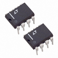
LT1126ACN8 Linear Technology, LT1126ACN8 Datasheet - Page 4

LT1126ACN8
Manufacturer Part Number
LT1126ACN8
Description
IC OP-AMP DECOMPENSAT DUAL 8-DIP
Manufacturer
Linear Technology
Datasheet
1.LT1126CN8PBF.pdf
(12 pages)
Specifications of LT1126ACN8
Amplifier Type
General Purpose
Number Of Circuits
2
Slew Rate
11 V/µs
Gain Bandwidth Product
65MHz
Current - Input Bias
7nA
Voltage - Input Offset
20µV
Current - Supply
2.6mA
Voltage - Supply, Single/dual (±)
±4 V ~ 18 V
Operating Temperature
-40°C ~ 85°C
Mounting Type
Through Hole
Package / Case
8-DIP (0.300", 7.62mm)
Lead Free Status / RoHS Status
Contains lead / RoHS non-compliant
Output Type
-
Current - Output / Channel
-
-3db Bandwidth
-
Available stocks
Company
Part Number
Manufacturer
Quantity
Price
Company:
Part Number:
LT1126ACN8
Manufacturer:
ONSemiconductor
Quantity:
2 000
Part Number:
LT1126ACN8#PBF
Manufacturer:
LINEAR/凌特
Quantity:
20 000
temperature range, otherwise specifications are at V
The
−40°C ≤ T
LT1126/LT1127
SYMBOL
V
∆V
I
I
V
CMRR
PSRR
A
V
SR
I
4
ELECTRICAL CHARACTERISTICS
SYMBOL
V
∆V
I
I
V
CMRR
PSRR
A
V
SR
I
Note 1: Absolute Maximum Ratings are those values beyond which the life
of a device may be impaired.
Note 2: Typical parameters are defined as the 60% yield of parameter
distributions of individual amplifiers; i.e., out of 100 LT1127s (or 100
LT1126s) typically 240 op amps (or 120) will be better than the indicated
specification.
Note 3: This parameter is 100% tested for each individual amplifier.
Note 4: This parameter is sample tested only.
Note 5: This parameter is not 100% tested.
Note 6: The inputs are protected by back-to-back diodes. Current limiting
resistors are not used in order to achieve low noise. If differential input
voltage exceeds ±1.4V, the input current should be limited to 25mA.
OS
B
S
OS
B
S
OS
CM
VOL
OUT
OS
CM
VOL
OUT
OS
OS
●
/∆T
/∆T
denotes the specifications which apply over the full operating temperature range, otherwise specifications are at V
A
≤ 85°C, unless otherwise noted. (Note 10)
PARAMETER
Input Offset Voltage
Average Input Offset Voltage Drift
Input Offset Current
Input Bias Current
Input Voltage Range
Common Mode Rejection Ratio
Power Supply Rejection Ratio
Large Signal Voltage Gain
Maximum Output Voltage Swing
Slew Rate
Supply Current Per Amplifier
PARAMETER
Input Offset Voltage
Average Input Offset Voltage Drift
Input Offset Current
Input Bias Current
Input Voltage Range
Common Mode Rejection Ratio
Power Supply Rejection Ratio
Large Signal Voltage Gain
Maximum Output Voltage Swing
Slew Rate
Supply Current Per Amplifier
CONDITIONS (Note 2)
LT1126
LT1127
(Note 5)
LT1126
LT1127
V
V
R
R
R
R
CONDITIONS (Note 2)
LT1126
LT1127
(Note 5)
LT1126
LT1127
V
V
R
R
R
R
CM
S
CM
S
L
L
L
L
L
L
L
L
= ±4V to ±18V
≥ 10kΩ, V
≥ 2kΩ, V
≥ 2kΩ
≥ 2kΩ (Notes 3, 7)
= ± 4V to ±18V
≥ 10kΩ, V
≥ 2kΩ, V
≥ 2kΩ
≥ 2kΩ (Note 7)
= ±11.5V
= ±11.4V
S
= ±15V, 0°C ≤ T
O
O
The
O
O
= ±10V
= ±10V
= ±10V
= ±10V
●
denotes the specifications which apply over the full operating
A
Note 7: Slew rate is measured in A
measured at ±5V.
Note 8: 0.1Hz to 10Hz noise can be inferred from the 10Hz noise voltage
density test. See the test circuit and frequency response curve for 0.1Hz to
10Hz tester in the Applications Information section of the LT1007 or
LT1028 datasheets.
Note 9: This parameter is guaranteed but not tested.
Note 10: The LT1126/LT1127 are designed, characterized and expected to
meet these extended temperature limits, but are not tested at –40°C and at
85°C. Guaranteed I grade parts are available. Consult factory.
≤ 70°C, unless otherwise noted.
●
●
●
●
●
●
●
●
●
●
●
●
●
●
●
●
●
●
●
●
●
●
●
●
●
●
●
●
± 11.4 ± 12.2
± 12.5 ± 13.6
± 11.5 ± 12.4
± 12.5 ± 13.7
MIN
109
112
4.0
1.5
7.5
MIN
107
111
3.5
1.2
7.3
LT1126AC
LT1127AC
LT1126AC
LT1127AC
± 8
± 15
TYP
35
40
0.3
6
7
125
125
15.0
3.5
10.5
2.7
TYP
40
45
0.3
15
15
124
124
12.0
3.2
10.2
2.8
± 50
± 35
MAX
140
160
1.0
40
50
3.4
MAX
120
140
1.0
25
35
3.3
V
= –10; input signal is ±1V, output
± 11.4 ± 12.2
± 12.0 ± 13.6
± 11.5 ± 12.4
± 12.0 ± 13.7
MIN
101
106
2.2
0.8
7.1
MIN
102
107
2.5
1.0
7.3
LT1126C
LT1127C
LT1126C
LT1127C
± 17
± 9
TYP
45
50
0.4
7
8
122
122
14.0
2.5
10.5
2.7
TYP
50
55
0.4
17
17
121
121
12.0
2.3
10.2
2.8
± 45
± 65
3.4
MAX
170
210
1.5
35
45
3.3
MAX
200
240
1.5
55
65
S
= ±15V,
UNITS
11267fa
UNITS
µV/°C
µV/°C
V/µV
V/µV
V/µV
V/µV
V/µs
V/µs
mA
mA
µV
µV
µV
µV
nA
nA
nA
dB
dB
nA
nA
nA
dB
dB
V
V
V
V


