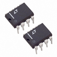
LT1126ACN8 Linear Technology, LT1126ACN8 Datasheet - Page 6

LT1126ACN8
Manufacturer Part Number
LT1126ACN8
Description
IC OP-AMP DECOMPENSAT DUAL 8-DIP
Manufacturer
Linear Technology
Datasheet
1.LT1126CN8PBF.pdf
(12 pages)
Specifications of LT1126ACN8
Amplifier Type
General Purpose
Number Of Circuits
2
Slew Rate
11 V/µs
Gain Bandwidth Product
65MHz
Current - Input Bias
7nA
Voltage - Input Offset
20µV
Current - Supply
2.6mA
Voltage - Supply, Single/dual (±)
±4 V ~ 18 V
Operating Temperature
-40°C ~ 85°C
Mounting Type
Through Hole
Package / Case
8-DIP (0.300", 7.62mm)
Lead Free Status / RoHS Status
Contains lead / RoHS non-compliant
Output Type
-
Current - Output / Channel
-
-3db Bandwidth
-
Available stocks
Company
Part Number
Manufacturer
Quantity
Price
Company:
Part Number:
LT1126ACN8
Manufacturer:
ONSemiconductor
Quantity:
2 000
Part Number:
LT1126ACN8#PBF
Manufacturer:
LINEAR/凌特
Quantity:
20 000
TYPICAL PERFOR
*See LT1115 data sheet for definition of CCIF testing
APPLICATIO S I FOR ATIO
Matching Specifications
In many applications the performance of a system de-
pends on the matching between two op amps, rather than
the individual characteristics of the two devices. The three
op amp instrumentation amplifier configuration shown in
this data sheet is an example. Matching characteristics are
not 100% tested on the LT1126/LT1127.
LT1126/LT1127
Expected Match
PARAMETER
V
Temperature Coefficient Match
Average Non-Inverting I
Match of Non-Inverting I
CMRR Match
PSRR Match
6
0.0001
OS
0.010
0.001
0.1
Match, ∆V
20
Total Harmonic Distortion
and Noise vs Frequency for
Inverting Gain
Z
V
A
MEASUREMENT BANDWITH
L
O
V
= 10Hz TO 80kHz
= 2k/15pF
= 20Vp-p
= –10, –100
100
OS
FREQUENCY (Hz)
LT1127
LT1126
A
V
B
B
= –100
U
1k
U
A
W
V
= –10
10k 20k
50% YIELD
1126-7 G07
A
U
0.35
126
127
20
30
6
7
W
CE
LT1126AM/AC
LT1127AM/AC
C
0.0001
0.010
0.001
HARA TERISTICS
0.1
20
Total Harmonic Distortion
and Noise vs Frequency for
Non-Inverting Gain
U
Z
V
A
MEASUREMENT BANDWITH
L
O
V
= 10Hz TO 80kHz
= 2k/15pF
= 20Vp-p
= +10, +100
98% YIELD
100
C
110
150
115
118
1.0
18
22
FREQUENCY (Hz)
A
V
= +100
Some specifications are guaranteed by definition. For
example, 70µV maximum offset voltage implies that mis-
match cannot be more than 140µV. 112dB (= 2.5µV/V)
CMRR means that worst case CMRR match is 106dB
(5µV/V). However, the following table can be used to
estimate the expected matching performance between the
two sides of the LT1126, and between amplifiers A and D,
and between amplifiers B and C of the LT1127.
1k
A
V
= +10
50% YIELD
10k 20k
1126-7 G08
123
127
0.5
30
50
7
8
LT1126M/C
LT1127M/C
0.0001
0.010
0.001
0.1
3k
Intermodulation Distortion
(CCIF Method)* vs Frequency
98% YIELD
Z
f (IM) = 1kHz
f
V
A
MEASUREMENT BANDWITH
130
180
112
114
O
1.5
25
30
L
O
V
= 10Hz TO 80kHz
= 13.5kHz
= 2k/15pF
= –10
= 20Vp-p
FREQUENCY (Hz)
10k
LT1126
UNITS
11267fa
µV/°C
1126-7 G09
µV
µV
nA
nA
dB
dB
20k


