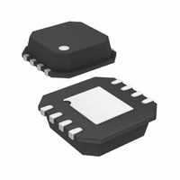
ADA4899-1YCPZ-R2 Analog Devices Inc, ADA4899-1YCPZ-R2 Datasheet - Page 14

ADA4899-1YCPZ-R2
Manufacturer Part Number
ADA4899-1YCPZ-R2
Description
IC OPAMP VF ULN ULDIST 8LFCSP
Manufacturer
Analog Devices Inc
Datasheet
1.ADA4899-1YCPZ-R7.pdf
(20 pages)
Specifications of ADA4899-1YCPZ-R2
Slew Rate
310 V/µs
Design Resources
High Speed, Precision, Differential AC-Coupled Drive Circuit for AD7625 (CN0080)
Amplifier Type
Voltage Feedback
Number Of Circuits
1
-3db Bandwidth
600MHz
Current - Input Bias
6µA
Voltage - Input Offset
35µV
Current - Supply
14.7mA
Current - Output / Channel
200mA
Voltage - Supply, Single/dual (±)
4.5 V ~ 12 V, ±2.25 V ~ 6 V
Operating Temperature
-40°C ~ 125°C
Mounting Type
Surface Mount
Package / Case
8-LFCSP
Op Amp Type
Voltage Feedback
No. Of Amplifiers
1
Bandwidth
600MHz
Supply Voltage Range
5V To 12V
Amplifier Case Style
LFCSP
No. Of Pins
8
Lead Free Status / RoHS Status
Lead free / RoHS Compliant
Output Type
-
Gain Bandwidth Product
-
Lead Free Status / RoHS Status
Lead free / RoHS Compliant, Lead free / RoHS Compliant
Other names
CRCW0201464RFNED
ADA4899-1
APPLICATIONS
UNITY-GAIN OPERATION
The ADA4899-1 schematic for unity-gain configuration is
nearly a textbook example (see Figure 46). The only exception is
the small 24.9 Ω series resistor at the noninverting input. The
series resistor is only required in unity-gain configurations;
higher gains negate the need for the resistor. In Table 4, it can be
seen that the overall noise contribution of the amplifier and the
24.9 Ω resistor is equivalent to the noise of a single 87 Ω resistor.
Figure 47 shows the small signal frequency response for the
unity-gain amplifier shown in Figure 46.
Table 4. Conditions: V
Gain
+1
−1
+2
+5
+10
R
0
100
100
200
453
F
(Ω)
V
IN
Figure 46. Unity-Gain Schematic
R
NA
100
100
49.9
49.9
24.9Ω
G
(Ω)
S
= ±5 V, T
R
24.9
0
0
0
0
+V
–V
S
(Ω)
S
S
A
0.1µF
= 25°C, R
0.1µF
−3 dB SS BW (MHz)
(25 mV p-p)
605
294
277
77
37
L
V
OUT
= 1 kΩ
Rev. B | Page 14 of 20
Slew Rate (V/μs)
(2 V Step)
274
265
253
227
161
RECOMMENDED VALUES FOR VARIOUS GAINS
Table 4 provides a handy reference for determining various
gains and associated performance. For noise gains greater than
one, the Series Resistor R
are kept low to minimize their contribution to the overall noise
performance of the amplifier.
Figure 47. Small Signal Frequency Response for Various Output Voltages
–12
–3
–6
–9
3
0
1
G = +1
R
L
= 100Ω
ADA4899-1 Voltage
Noise (nV/√Hz)
1
2
2
5
10
10
S
is not required. Resistors R
FREQUENCY (MHz)
200mV p-p
100mV p-p
100
50mV p-p
1000
Total Voltage
Noise (nV/√Hz)
1.2
2.7
2.7
6.5
13.3
25mV p-p
F
and R
10000
G


