ADA4899-1YCPZ-R2 Analog Devices Inc, ADA4899-1YCPZ-R2 Datasheet - Page 3
ADA4899-1YCPZ-R2
Manufacturer Part Number
ADA4899-1YCPZ-R2
Description
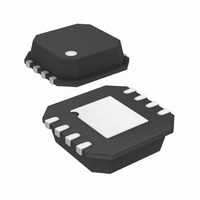
IC OPAMP VF ULN ULDIST 8LFCSP
Manufacturer
Analog Devices Inc
Datasheet
1.ADA4899-1YCPZ-R7.pdf
(20 pages)
Specifications of ADA4899-1YCPZ-R2
Slew Rate
310 V/µs
Design Resources
High Speed, Precision, Differential AC-Coupled Drive Circuit for AD7625 (CN0080)
Amplifier Type
Voltage Feedback
Number Of Circuits
1
-3db Bandwidth
600MHz
Current - Input Bias
6µA
Voltage - Input Offset
35µV
Current - Supply
14.7mA
Current - Output / Channel
200mA
Voltage - Supply, Single/dual (±)
4.5 V ~ 12 V, ±2.25 V ~ 6 V
Operating Temperature
-40°C ~ 125°C
Mounting Type
Surface Mount
Package / Case
8-LFCSP
Op Amp Type
Voltage Feedback
No. Of Amplifiers
1
Bandwidth
600MHz
Supply Voltage Range
5V To 12V
Amplifier Case Style
LFCSP
No. Of Pins
8
Lead Free Status / RoHS Status
Lead free / RoHS Compliant
Output Type
-
Gain Bandwidth Product
-
Lead Free Status / RoHS Status
Lead free / RoHS Compliant, Lead free / RoHS Compliant
Other names
CRCW0201464RFNED


SPECIFICATIONS WITH ±5 V SUPPLY
T
Table 1.
Parameter
DYNAMIC PERFORMANCE
NOISE/DISTORTION PERFORMANCE
DC PERFORMANCE
INPUT CHARACTERISTICS
DISABLE PIN
OUTPUT CHARACTERISTICS
POWER SUPPLY
A
–3 dB Bandwidth
Bandwidth for 0.1 dB Flatness
Slew Rate
Settling Time to 0.1%
Harmonic Distortion, HD2/HD3 (dBc)
Input Voltage Noise
Input Current Noise
Input Offset Voltage
Input Offset Voltage Drift
Input Bias Current
Input Resistance
Input Capacitance
Input Common-Mode Voltage Range
Common-Mode Rejection Ratio
DISABLE Input Threshold Voltage
Turn-Off Time
Turn-On Time
Input Bias Current
Output Overdrive Recovery Time (Rise/Fall)
Output Voltage Swing
Short-Circuit Current
Off Isolation
Operating Range
Quiescent Current
Quiescent Current (Disabled)
Positive Power Supply Rejection Ratio
Negative Power Supply Rejection Ratio
Input Bias Current Drift
Input Bias Offset Current
Open-Loop Gain
= 25°C, G = +1, R
L
= 1 kΩ to ground, unless otherwise noted.
Conditions
V
V
G = +2, V
V
V
f
f
f = 100 kHz
f = 100 kHz, DISABLE pin floating
f = 100 kHz, DISABLE pin = +V
DISABLE pin floating
DISABLE pin = +V
Differential mode
Common mode
Output disabled
50% of DISABLE voltage to 10% of V
50% of DISABLE voltage to 90% of V
DISABLE = +V
DISABLE = −V
V
R
R
Sinking/sourcing
f = 1 MHz, DISABLE = −V
DISABLE = −V
+V
−V
C
C
OUT
OUT
OUT
OUT
IN
L
L
= 500 kHz, V
= 10 MHz, V
= 1 kΩ
= 100 Ω
S
S
V
V
= −2.5 V to +2.5 V, G = +2
= 4 V to 6 V (input referred)
= −6 V to −4 V (input referred)
IN
IN
= 25 mV p-p
= 2 V p-p
= 5 V step
= 2 V step
= 0.5 V
= 0.5 V
OUT
= 2 V p-p
S
S
S
OUT
Rev. B | Page 3 of 20
OUT
(enabled)
(disabled)
= 2 V p-p
= 2 V p-p
S
S
S
OUT
OUT
,
,
Min
82
98
−3.65 to +3.65
−3.13 to +3.15
4.5
84
87
Typ
600
80
35
310
50
−123/−123
−80/−86
1.0
2.6
5.2
35
5
−6
−0.1
3
0.05
85
4
7.3
4.4
−3.7 to +3.7
130
<2.4
100
40
17
−35
30/50
−3.7 to +3.7
−3.25 to +3.25
160/200
−48
14.7
1.8
90
93
ADA4899-1
Max
230
−12
−1
21
−44
16.2
2.1
0.7
12
Unit
MHz
MHz
MHz
V/μs
ns
dBc
dBc
nV/√Hz
pA/√Hz
pA/√Hz
μV
μV/°C
μA
μA
nA/°C
μA
dB
kΩ
MΩ
pF
V
dB
V
ns
ns
μA
μA
ns
V
V
mA
dB
V
mA
mA
dB
dB
Related parts for ADA4899-1YCPZ-R2
Image
Part Number
Description
Manufacturer
Datasheet
Request
R

Part Number:
Description:
IC OPAMP VF ULN ULDIST 8SOIC
Manufacturer:
Analog Devices Inc
Datasheet:
Part Number:
Description:
IC,Operational Amplifier,SINGLE,BIPOLAR,SOP,8PIN,PLASTIC
Manufacturer:
Analog Devices Inc
Datasheet:

Part Number:
Description:
IC,Operational Amplifier,SINGLE,BIPOLAR,LLCC,8PIN,PLASTIC
Manufacturer:
Analog Devices Inc
Datasheet:
Part Number:
Description:
IC,Operational Amplifier,SINGLE,BIPOLAR,LLCC,8PIN,PLASTIC
Manufacturer:
Analog Devices Inc
Datasheet:
Part Number:
Description:
IC,Operational Amplifier,SINGLE,BIPOLAR,SOP,8PIN,PLASTIC
Manufacturer:
Analog Devices Inc
Datasheet:

Part Number:
Description:
Unity-Gain Stable, Ultralow Distortion, 1 nV/?Hz Voltage Noise, High Speed Op Amp
Manufacturer:
Analog Devices
Datasheet:

Part Number:
Description:
ADA4899-1YRD-EBZ_A00973_EB-O8-REDF-1Z
Manufacturer:
Analog Devices Inc
Part Number:
Description:
AD4899-1YCP-EBZ_A00975_EB-O8CP33-1Z
Manufacturer:
Analog Devices Inc

Part Number:
Description:
Unity-Gain Stable, Ultralow Distortion, 1 nV/?Hz Voltage Noise, High Speed Op Amp
Manufacturer:
AD [Analog Devices]
Datasheet:

Part Number:
Description:
±1.7g Dual-Axis IMEMS Accelerometer Evaluation Board
Manufacturer:
Analog Devices Inc
Datasheet:
Part Number:
Description:
Inertial Sensor Evaluation System
Manufacturer:
Analog Devices Inc
Datasheet:
Part Number:
Description:
Manufacturer:
Analog Devices Inc
Datasheet: